6.6kW High Power Density Bi-directional EV On-Board Charger
Article
Abstract
This paper presents a Silicon Carbide (SiC) MOSFET-based 6.6 kW bi-directional Electric Vehicle (EV) on-board charger (OBC), with high efficiency and high power density. A digital controlled prototype with a switching frequency of 67kHz for CCM totem pole PFC, and 150kHz-300kHz for a CLLC resonant converter is demonstrated with 54W/in3 power density exceeding 96.5% in peak efficiency. In order to achieve a high power density, all Silicon Carbide MOSFETs are mounted on a tooled AL heat sink, with all magnetics potted internally. MOSFETs and magnetics meet thermal requirements on a 65°C cooling plate.
Introduction
As the world moves towards cleaner fuel alternatives, the EV transportation segment is experiencing rapid growth. Further, EVs equipped with a sufficient battery capacity have potential application in supporting standalone loads (V2L), and supplement grid power (V2G). Thus, the design trend of the EV’s OBC is a transition to bi-directional operation capacity.
In order to optimize EV space and weight, OBC design requires high power density and maximized efficiency. The bi-directional OBC consists of a bi-directional AC-DC converter followed by an isolated bi-directional DC-DC converter. The conventional LLC resonant converter was originally proposed as a solution to improve the efficiency of the DC-DC converter [1]. However, given its unidirectional design, in reverse operation mode voltage gain of the converter was limited, thus the intended advantages of the converter could not be realized [2] – [3]. Subsequently, a bi-directional CLLC resonant converter [3] – [4] was selected in this paper for the DC-DC stage, as it was found to provide high efficiency and a wide output voltage range in both charging and discharging modes.
A conventional PFC boost converter is the most popular single-phase PFC topology. Unfortunately, conduction losses of the diode bridge rectifier are not efficient, nor does it support bi-directional operation [5]. Next, the totem pole bridgeless PFC boost converter was considered in order to reduce diode numbers and increase efficiency [6], [7]. However, reverse recovery of the body diode of silicon MOSFETs resulted in high power losses in continuous conduction mode (CCM) making them impractical for high power applications. Following, insulated gate bipolar transistors (lGBT) paralleled with Silicon Carbide Schottky diodes were considered to replace silicon MOSFETs in CCM totem pole PFC and CLLC converters [8]. Sadly, the practical switching frequency is limited due to the high switching loss of IGBT. Further, the objective of a lighter, more power-dense OBC is negatively affected by the weight and size of the magnetics and resonant tank, as well from the additional anti-parallel SiC diodes.
Owing to the favorable reverse recovery performance of the body diode of SiC MOSFETs, interleaved CCM totem pole PFC is enabled as the front-end stage of a 3.3 kW OBC [9]. With its ability to achieve high-power density and simple control, a single-phase single choke CCM totem pole PFC solution is selected for this paper.
For thermal management, MOSFETs in a TO-247 package are normally reverse-assembled on the PCB in OBC applications. They are then mounted on a flat cooling baseplate. However, when the MOSFETs are bent down PCB area is increased, thus, negatively impacting the overall power density of the system.
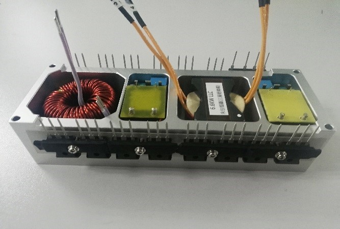
The proposed method is utilization of a tooled heat sink which accommodates both semiconductors and magnetics. Power semiconductors are mounted on the outer side of the heat sink, allowing for vertical MOSFET assembly, thus reducing PCB footprint. Magnetics are then potted using a thermal compound inside the slots of the heat sink. Thermal resistance from the tooled aluminum heat sink to the system cooling baseplate is low. As an example, a Silicon Carbide MOSFET-based 6.6 kW bi-directional OBC is designed. The experimental results for the converter operating in the charging mode and discharging mode manifest both high efficiency and high power density.
The Specifications and Architecture of a Bi-Directional OBC
Bidirectional OBC Specifications
Table 1 provides the major design specifications of the 6.6kW bi-directional on-board charger.
AC Input/output Voltage | 90Vac – 265Vac |
DC Input/output Voltage | 250V – 450VDC |
Rated Power | 6.6kW charging; 3.3kW discharging |
Peak Efficiency | >96.5% charging and discharging |
Baseplate Temperature | 65°C |
PCBA Dimensions | 220mm × 180mm × 50mm |
Block Diagram, DC-link Voltage and Switching Frequency Selection
Figure 1 shows the system block diagram of the bidirectional OBC.
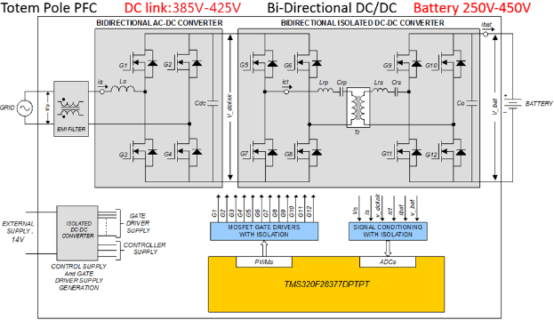
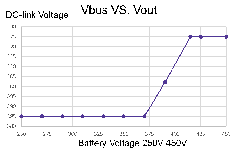
An OBC design with a 500V-840V variable DC-link for 250V-450V battery voltage based on 1200V Silicon Carbide MOSFET is demonstrated [10]. Overall efficiency of the OBC is optimized, however, 1200V SiC MOSFET cost is high. Power loss of PFC MOSFET and PFC choke is also elevated with high DC-link voltage. The size of the DC link capacitors and PFC choke are larger for the 840V design. 450 V Ecap, which is commonly used in the industry, is optimized with smaller size and low cost. When using 450V Ecaps not in serials, the DC-link voltage is maxed at 425V. A 385V DC link is the minimum voltage to maintain adequate power for an AC input, up to 265Vac. In this design, as shown in Fig. 2, the DC-link voltage of the OBC is variable from 385V to 425V, to allow the CLLC converter a smaller required gain range and better efficiency over the 250V-450V battery voltage range compared to a fixed 400V DC-link in charging mode.
To attain a balance between power density, efficiency, thermal performance, and conducted EMI, 67kHz is selected for the switching frequency of the high frequency half bridge Q1 and Q3 of the totem pole PFC.
To achieve high power density and efficiency, 200kHz is selected for the CLLC converter resonant frequency, and 150kHz to 300kHz for the frequency range. It is a trade-off between power density, efficiency and thermal performance. For a light load at low output voltage, combined PFM and phase shift control are applied in this design.
Power MOSFET Selection
A fast reverse recovery body diode is required for efficiency and reliability for both the CCM totem pole PFC and bidirectional CLLC resonant converter. A smaller Coss is preferred for high-frequency hard-switching operations for the totem pole PFC. A smaller Coss is also critical for achieving zero voltage switching (ZVS) with a lower magnetizing current and a shorter blanking time for the CLLC resonant converter. With reduced magnetizing current, the conduction loss and turn-off switching loss of the MOSFET can be minimized. That is important for optimizing the efficiency of the CLLC converter, particularly at high frequencies. The maximum DC-link voltage is 425V and the battery is 450V. In consideration of voltage de-rating reliability requirements, a 650V SiC MOSFET is preferred in the OBC application.
In order to deliver 6.6kW output power, C3M0060065D 650V 60mohm SiC MOSFET in TO-247 package, two parts in parallel are selected for the high frequency half bridge of CCM totem pole PFC. A single C3M0060065D is selected for the low frequency half bridge of PFC and both the DC-link side and the battery side of the CLLC resonant converter.
Digital Controller Selection
Digital controller TMS320F28377D was chosen to implement the flexible control of both the totem pole PFC and CLLC converter of the OBC in charging and discharging modes. As shown in Fig. 1, TMS320F28377D provides 12 independent PWMs G1-G12 to MOSFETs Q1-Q12 for the totem pole PFC and CLLC converter. The digital controller also handles the real-time CAN communication, start-up sequence, OCP, OTP, UVP and OVP.
Magnetics and Key Parameters
The PFC choke is designed to keep the totem pole PFC current ripple under 40%. The maximum current ripple occurs at low line, high battery voltage and full load. The minimum required inductance is 75uH, which is calculated in Eq. (1).
Considering the permeability degrade with DC bias, 230uH is selected for the PFC choke without DC bias. To get a balance between core loss and DC bias capability, the choke is fabricated with 2 stacks of KAM185-060A cores [11]. The winding consists of 36 turns of 2-strand AWG-13 magnet wires.
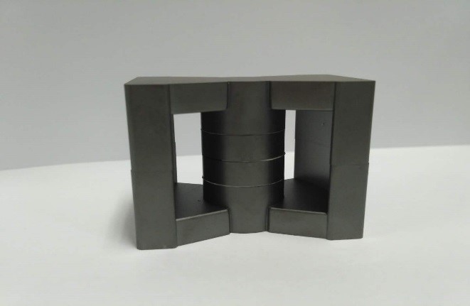
The main transformer of the CLLC converter is designed to meet the requirements of both 450V/14.67A and 366V/18A output. The max flux density and core loss are designed for and verified at 425V DC-link and 450V/14.67A output. The winding wire size is designed for maximum current conditions with a 366V/18A output. With a bobbin-less design, the window area of the core can be fully utilized. Next, a PQ5040 core using 3C97 material is selected for the 6.6kW CLLC converter. To meet the gain range requirements for 250V-450V battery in both charging and discharging mode, a 1:1 turn ratio is selected. As shown in Fig.3, to minimize the power loss caused by eddy current, the distributed air gaps are designed at center leg of the core. 14 turns triple isolated 400-strand AWG-38 liz wire is designed as both the primary winding and the battery side winding. A 60uH magnetizing inductance is selected to ensure the ZVS of CLLC MOSFETs.
Key design parameters are shown in Table 2.
ACDC Choke | 230 uH | Resonant choke primary | 8.8 uH |
ACDC switching frequency 67 kHz | 67 kHz | Resonant cap primary | 74.8 nF |
Resonant frequency | 200 kHz | Resonant choke secondary | 8.8 uH |
DC-link cap | 1800 uF | Resonant cap secondary | 74.8 nF |
Hardware Implementation and Test Results
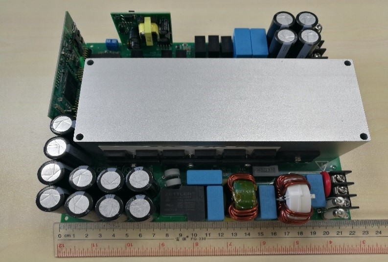
As shown in Fig. 4, (including the input EMI filter, totem pole PFC, CLLC resonant converter, control board, and auxiliary power board), a 6.6kW bidirectional OBC prototype is built to verify the design. The PCBA dimensions are 220mm × 180mm × 50mm.
Figure 5 shows the integrated heatsink for both the semiconductors and magnetics. The power semiconductors are mounted on the outer side of the heatsink. The magnetics are potted by thermal compound inside the slots of the same heatsink. C3M0060065D engineering samples are used in the prototype.
Key Waveforms
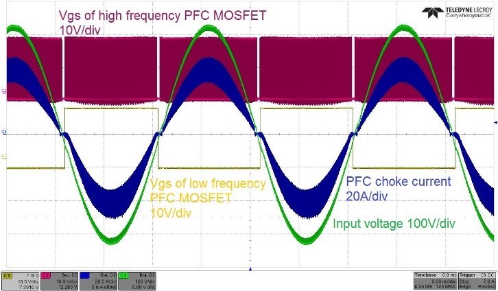
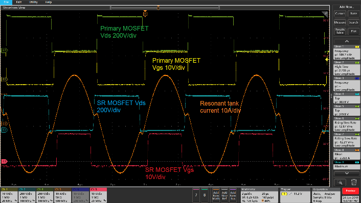
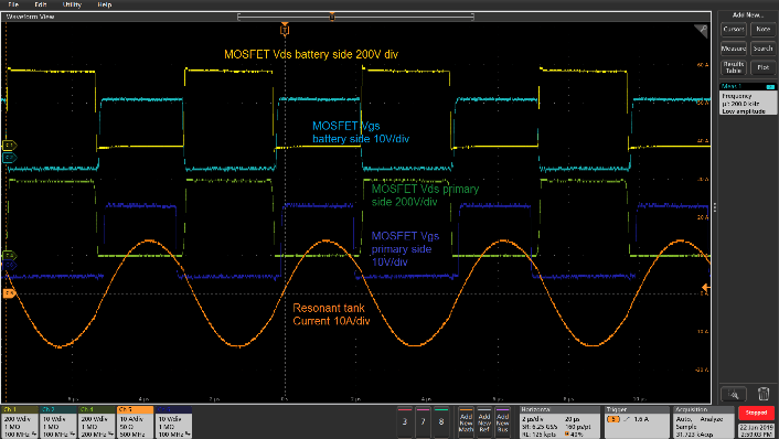
The testing waveforms of totem pole PFC and CLLC stage in charging mode under 380V battery voltage, 230Vac input and full load are shown in Fig. 6 and Fig. 7 respectively.
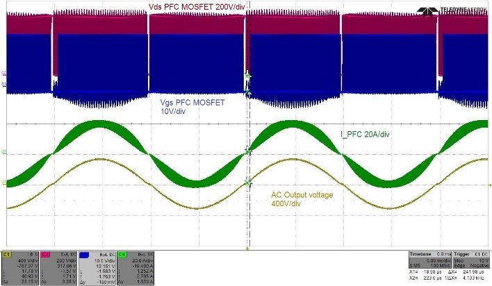
The testing waveforms of DC/AC and DC/DC stage in discharging mode under 380V battery voltage input and 220Vac output are shown in Fig. 8 and Fig.9 respectively.
Efficiency Test Result
The efficiency of the CCM totem pole PFC, DC/DC stage and the entire unit in charging mode at 230Vac input are shown in Figs. 10, 11 and 12 respectively. With a lower DC-link voltage, the totem pole PFC efficiency is higher. The unit level peak efficiency in charging mode exceeds 96.5%. C3M0060065D engineering samples are used in the prototype.
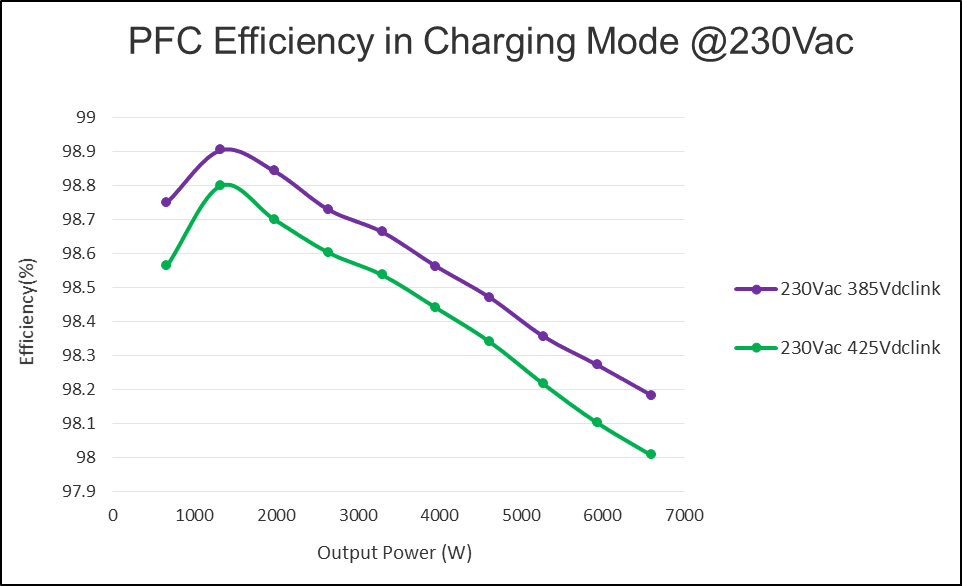
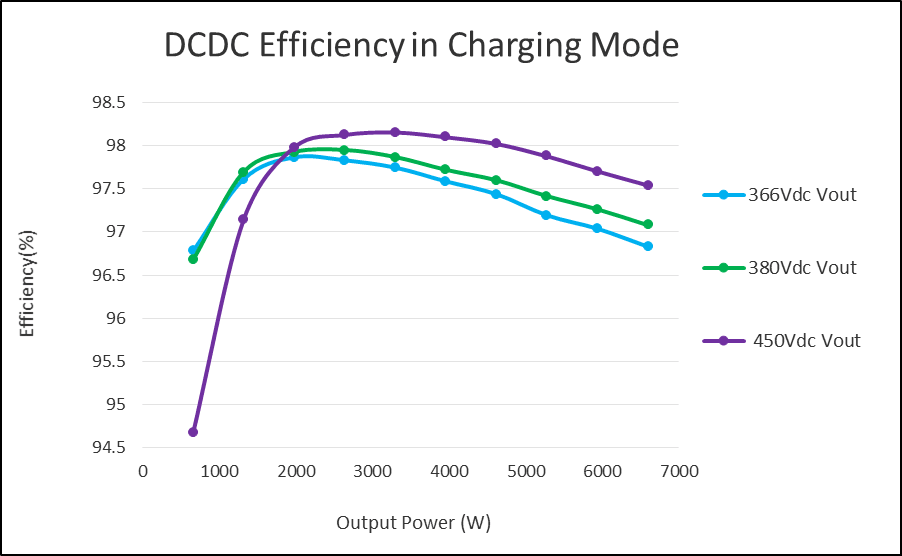
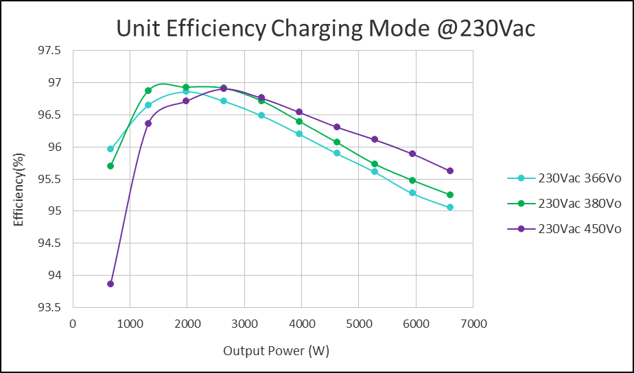
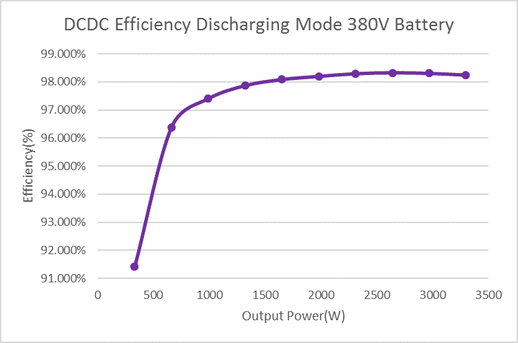
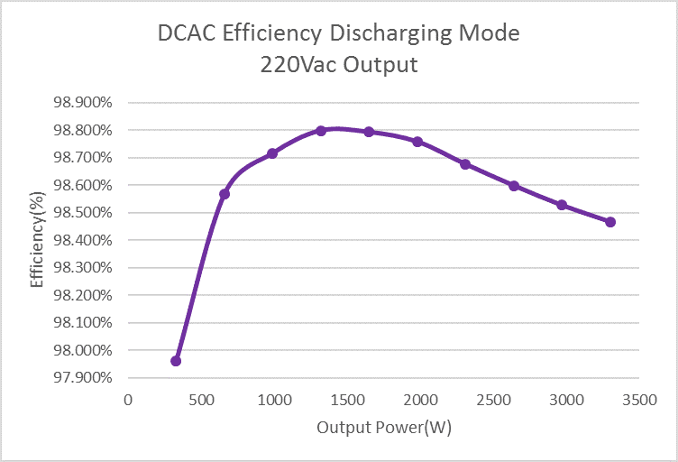
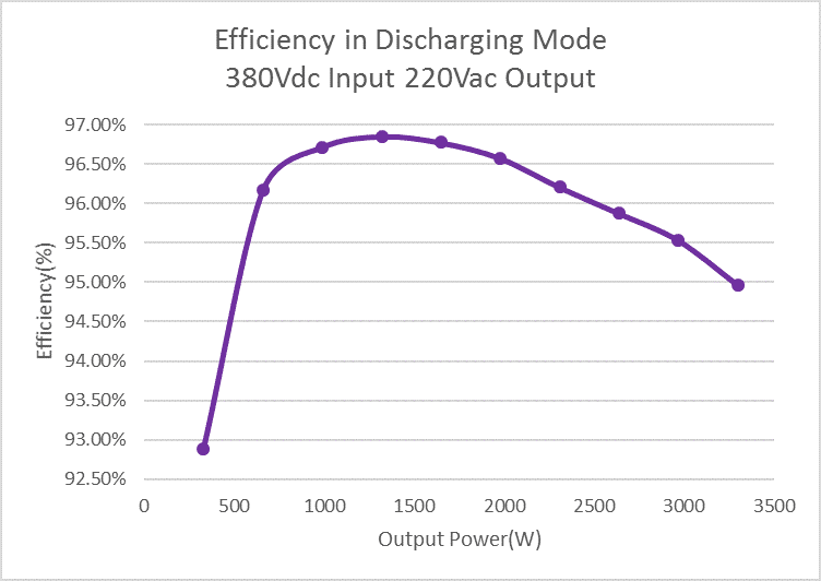
Figure 13 shows the efficiency of DCDC in discharging mode at 380V battery voltage. Figure 14 shows the efficiency of DCAC stage in discharging mode for 220Vac output. Figure 15 shows the unit level efficiency in discharging mode for 220Vac output. The output power in the efficiency test is up to 3.3kW in discharging mode here. The unit level peak efficiency in discharging mode is also above 96.5%.
Thermal Test Result
In the thermal test of the prototype, forced air cooling is applied to the cooling base plate at bottom side to get a 65⁰C cooling plate to simulate the thermal condition in an OBC application. There is no air flow to the power MOSFETs. C3M0060065D engineering samples are used in the prototype. MOSFETs in the CLLC resonant converter operate in the worst case thermal condition with a 366V/18A load. The totem pole PFC converter operates in the worst case thermal condition with a 450V/14.67A load. So, the thermal test was performed at a low line 215Vac and full load 6.6kW with 366V/18A and 450V/14.67A in charging mode. T-type thermal couplers and KEYSIGHT 34972A acquisition unit are used to measure the case temperature of components.
Description | Rth j-c (c/w) | Calculated Power loss(watts) | Measured Case Temp. (°C) | Calculated Junction Temp. (°C) |
|---|---|---|---|---|
366V output 6.6kW | ||||
PFC MOSFET | 1.58 | 18 | 97.9 | 126.3 |
CLLC MOSFET | 1.58 | 18 | 95.8 | 125.4 |
CLLC SR MOSFET | 1.58 | 16.8 | 87.8 | 114.4 |
L_PFC | NA | 13.9 | 89.2 | NA |
T_DCDC | NA | 13.8 | 114.9 | NA |
450V output 6.6kW | ||||
PFC MOSFET | 1.58 | 18.3 | 100.5 | 129.4 |
CLLC MOSFET | 1.58 | 17.8 | 92.5 | 120.6 |
CLLC SR MOSFET | 1.58 | 11 | 86.8 | 104.2 |
L_PFC | NA | 15.1 | 91.4 | >NA |
T_DCDC | NA | 19.5 | 123.1 | NA |
Table 3: Thermal Test Results. |
The thermal test results are shown in Table 3. The junction temperature is calculated based on the measured case temperature, the thermal resistance of the MOSFET and the calculated component power loss. The target maximum junction temperature of C3M0060065D is 175°C. Refer to the test result, the max junction temperature of the SiC MOSFETs is 129.4°C at worst case in the application. So, we can get the conclusion that, based on the integrated heat sink proposal, all of the MOSFETs meet thermal de-rating requirement in this high-power density design.
Conclusions and Future Work
In this paper, a 6.6 kW bi-directional OBC on SiC MOSFET is designed and evaluated. The DC-link voltage range is optimized to 385V to 425V per a common battery voltage range of 250V to 450V for an OBC. A prototype based on engineering samples of 650V 60mohm SiC MOSFET C3M0060065D is built to verify the performance and thermal integrity of the design. 54 W/in3 power density and above 96.5% peak efficiency in both charging and discharging mode are demonstrated by the prototype with 67 kHz for the CCM totem pole PFC converter and 150-300 kHz for the CLLC resonant converter. By integrating the power semiconductors and power magnetics on the same tooled heat sink, high power density and high efficiency can be achieved in bi-directional high power conversion applications such as OBC for EV, owing to the low power loss of 650V SiC MOSFET. The future work is to improve thermal management for transformer to reduce its temperature rise.
References
- Bo Yang; F.C. Lee; A.J. Zhang; Guisong Huang: LLC resonant converter for front end DC/DC conversion, Proc. IEEE APEC, 2002, vol. 2, pp. 1108 – 1112.
- Sihun Yang; Masahito Shoyama; Toshiyuki Zaitsu; Junichi Yamamoto; Seiya Abe; Tamotsu Ninomiya: Detail operating characteristics of Bi-directional LLC resonant converter, ICRERA, 2012, pp. 1 – 6.
- Wei Chen; Ping Rong; Zhengyu Lu: Snubberless Bidirectional DC–DC Converter With New CLLC Resonant Tank Featuring Minimized Switching Loss, Industrial Electronics, IEEE Transactions on, vol. 57, no. 9, 2010, pp. 3075 – 3086
- Zheng Lv; Xiangwu Yan; Yukang Fang; Lei Sun: Mode analysis and optimum design of bidirectional CLLC resonant converter for high-frequency isolation of DC distribution systems, ECCE, 2015, pp. 1513 – 1520.
- J. P. M. Figuerido, F. L. Tofili, and B. L. A. Silva: A review of single-phase PFC topologies based on the boost converter, in Proc. IEEE Int. Conf. Indus. Appl., Sao Paulo, Brazil, Nov. 2010, pp. 1 – 6.
- J. W. Lim and B. H. Kwon: A power factor controller for single phase PWM rectifiers, IEEE Trans. Ind. Electron., vol. 46, no. 5, pp. 1035–1037, Oct. 1999.
- B. Su, J. M. Zhang, and Z.Y. Lu: Totem-pole boost bridgeless PFC rectifier with simple zero-current detection and full-range ZVS operating at the boundary of DCM/CCM, IEEE Trans. on Power Electron., vol. 26, no. 2, pp. 427-435, Feb. 2011.
- Jih-Sheng Lai; Lanhua Zhang; Zaka Zahid; Nan-Hsiung Tseng; Chi-Seng Lee; Chin-Hone Lin: A high-efficiency 3.3-kW bidirectional on-board charger, 2015 IEEE 2nd International Future Energy Electronics Conference (IFEEC), pp. 1 - 5.
- Yichao Tang; Weisheng Ding; Alireza Khaligh: A bridgeless totem-pole interleaved PFC converter for plug-in electric vehicles, 2016 IEEE Applied Power Electronics Conference and Exposition (APEC), pp. 440 - 445.
- Bin Li; Fred C. Lee; Qiang Li; Zhengyang Liu: Bi-directional on-board charger architecture and control for achieving ultra-high efficiency with wide battery voltage range, APEC 2017, pp. 3688 - 3694.
- KAM, https://www.kda.com.cn/products/tncfx-376.html