Application of SiC MOSFETs in 6.6kW High-Frequency High-Power-Density Power Converter
Article
Abstract
This paper presents the application of Silicon Carbide (SiC) devices in a high-frequency LLC resonant DC/DC converter which can be used in bus converters, EV chargers, server powers, and energy storage. With high switching frequencies, the leakage inductance of the LLC transformer can be used as the resonant inductor, resulting in 50% reduction in volume and weight, and 30% decrease in power loss of the magnetic components at 500 kHz and 6.6 kW/400 V output. Experimental results have demonstrated the superb performance of SiC power devices over Si-based counterparts with a near 98.5% peak converter efficiency at 500 kHz in a converter with 400 V/16 A output.
Introduction
High efficiency and high power density has been a continuing demand for switching mode power supplies [1]. The technology development and applications of wide bandgap (WBG) power devices, such as Silicon Carbide (SiC) devices, have enabled themselves as the promising substitutions for traditional Silicon (Si) devices in a variety of applications. Due to its superior switching speed and low switching loss along with low temperature dependency of turn-on resistance (RDS_ON), higher efficiency, higher power density, and improved robustness and reliability can be achieved [2-5]. This work will demonstrate the performance of SiC MOSFETs in a 6.6 kW DC/DC converter at 500 kHz up to 1.5 MHz. The main benefits of high-frequency operation are smaller transformer and EMI filter, and an integrated resonant inductor into the transformer, which further reduces the size of the converter. Compared to traditional 100 kHz – 200 kHz DC/DC converters, the circuit running at 500 kHz exhibits a 50% volume and weight reduction of the magnetic parts with a peak efficiency near 98.5% for an LLC converter (400V/16A output). Thanks to a much less severe cross-talk due to ZVS, the SiC MOSFETs can operate reliably even without negative bias drive voltage, which reduces the driving circuit cost. Practical design guidelines for high-frequency operation, such as PCB layout, magnetic-core material and airgap selection, winding-wire size and construction, resonant capacitor selection, etc., along with test results, will be presented in this paper.
Simulations of High-Frequency LLC DC/DC Converters
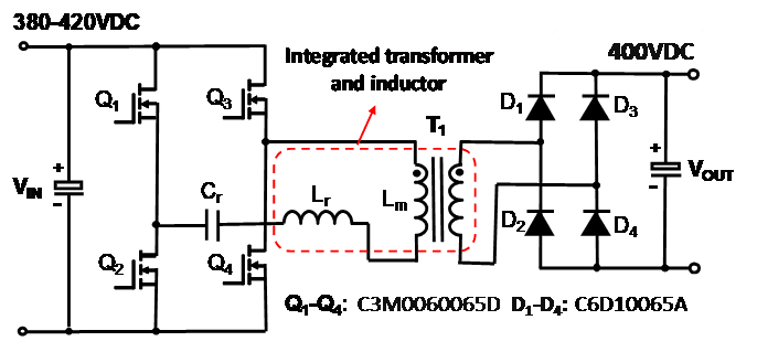
Simulations using LTspice were conducted to study the performance of the SiC MOSFETs along with factors affecting the converter efficiency. Fig. 1 shows the simplified schematic diagram of a full-bridge LLC DC/DC converter. At 500 kHz switching frequency with a magnetizing inductance Lm = 30 μH, the simulated total power loss of the four primary switches is 80.24 W (20.06 W for each) and the overall efficiency reaches 98.11% with diodes for output rectifiers thanks to ZVS turn-on of all the primary switches.
A large magnetizing inductance Lm can reduce the magnetizing current and lower the conduction loss of the primary switches; however, the value of Lm also needs to provide a sufficient magnetizing current to totally discharge the drain-source capacitors and ensure primary switch ZVS turn-on during the dead-time. Therefore, Lm should satisfy (1) [6].
Where, td is the dead-time between the two gate drive signals for the upper and lower switches, fs is the switching frequency, and CTotal is the total capacitance, including the drain-source capacitance of the primary switch, parasitic capacitance of the PCB, and reflected capacitance of the secondary-side diodes. For a given dead-time td, Lm can be optimally designed based on (1) and the high efficiency at normal operation can be achieved.
Design considerations
Design of LLC transformer
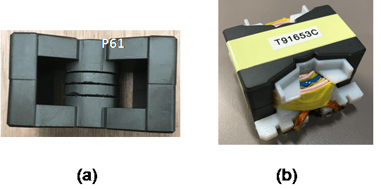
After the maximum magnetizing inductance is calculated using (1), the magnetic core material, airgap, and wire sizes need to be carefully considered for high-frequency operation, otherwise extreme power loss will result, causing unexpected failure of the transformer due to overheating. Among the core materials suitable for high frequencies, P61 from Acme was chosen for its low power loss and easy availability of core shapes for high power applications with a switching frequency range from 500 kHz to 1MHz. A PQ50/28 core was used for initial testing. Both the primary (φ0.05mm × 360 ×4) and secondary windings (φ0.05mm × 3400 × 32 TIW) employed served Litz wires with 9 turns for each. To reduce the copper loss induced by the fringing magnetic flux near the airgap, three distributed airgaps instead of one large airgap were used, as shown in Fig. 2.
PCB layout
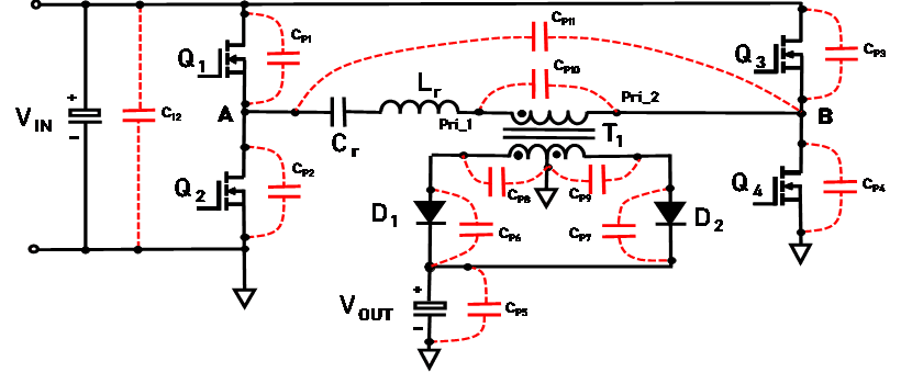
PCB layout plays a critical role in EMI, signal integrity, and circuit efficiency and operation – especially with high-frequency LLC converters. Fig. 3 shows the parasitic capacitances present within the experimental PCBs (Ver. 1 and Ver. 2) for an LLC converter. Ver. 1 PCB was done with large copper areas intended for power loss reduction of the PCB traces and cancelling of the magnetic fields of the current loops; however, large parasitic capacitances as shown in Table I were created because of the big overlapping area between different copper layers. Ver. 2 PCB has much smaller copper and overlapping areas for traces, which results in significantly lower parasitic capacitances. The parasitic capacitances were measured using a handheld LRC meter on a bare PCB (no parts were populated). In an LLC circuit, large parasitic capacitances across the switches (CP1-CP4), transformer windings (CP8-CP10), and mid-points of the primary side (CP11) will cause an undesired efficiency drop (measured 0.8% drop and 26 W more power loss as shown in Table 1). Therefore, a trade-off between the copper loss reduction and parasitic effects needs to be made.
Table 1 Measured Parasitic Capacitances (Unit:pF) and Performance Comparison
PCB Version | CP1 | CP2 | CP3 | CP4 | CP5 | CP6 | CP7 | CP8 | CP9 | CP10 | CP11 | CP12 | Efficiency (%) | Power Loss (W) |
|---|---|---|---|---|---|---|---|---|---|---|---|---|---|---|
Ver. 1 | 315 | 390 | 343 | 420 | 4860 | 534 | 620 | 535 | 598 | 508 | 896 | 1385 | 95.71 | 141.57 |
Ver. 2 | 17 | 22 | 25 | 28 | 4731 | 528 | 516 | 589 | 575 | 11 | 13 | 308 | 96.50 | 115.50 |
Experimental Results
Fig. 4 shows the picture of the prototype with a power density of 128 W/in3 using SiC MOSFETs (C3M0060065D, 60 mΩ650 V) in TO-247-3 packages for the primary switches and SiC diodes (C6D10065A, 10 A/650 V) in TO-220 packages for the output rectifiers. Due to the high-frequency operation, the leakage inductance (1μH) of the main transformer was used for the resonant inductor without the need for an external inductor. A TI DSP-based control card (TMDSCNCD280049C) was used to generate the desired gate drive signals for either open-loop operation or closed-loop operation to regulate the output voltage. An auxiliary power supply (CRD-15DD17P by Wolfspeed) generates the power for the control circuit and the gate drivers.
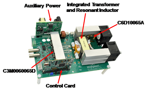
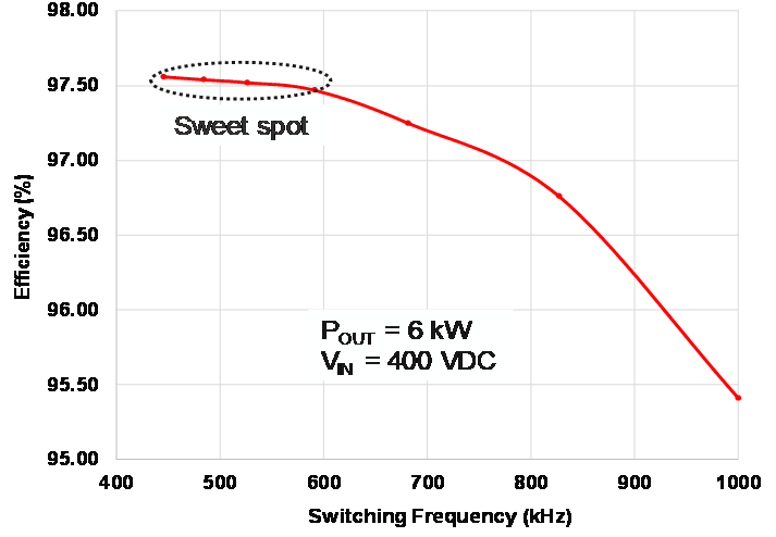
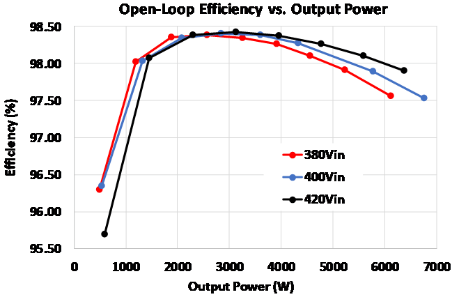
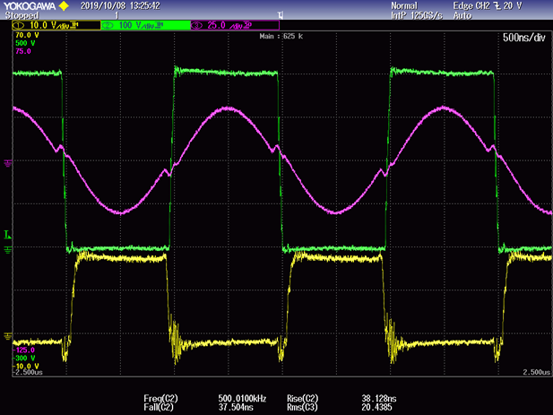
Fig. 5 shows the measured efficiency vs. switching frequency for 400V/16A DC output. The optimum switching frequency ranges from 500 kHz to 650 kHz without considerable efficiency drop. The decrease in efficiency as the switching frequency increases is mainly due to increased frequency-dependent copper losses and core loss in the LLC transformer [7] - [9] and PCB trace loss. The measured power loss due to the gate drive increases by 2.2W from 500 kHz to 1 MHz while there is a 3.5W power loss increase for each MOSFET (from 20.06 W to 23.56 W simulated). Fig. 6 shows the plots of efficiency vs. output power in open-loop operation. A peak efficiency of about 98.5% is achieved at half load (~3 kW). Fig. 7 shows the captured gate-source and drain-source waveforms of the primary-side upper switch along with the primary-side resonant current waveform at 550 kHz and 400 V input.
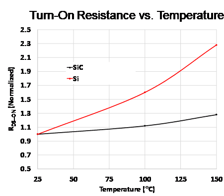
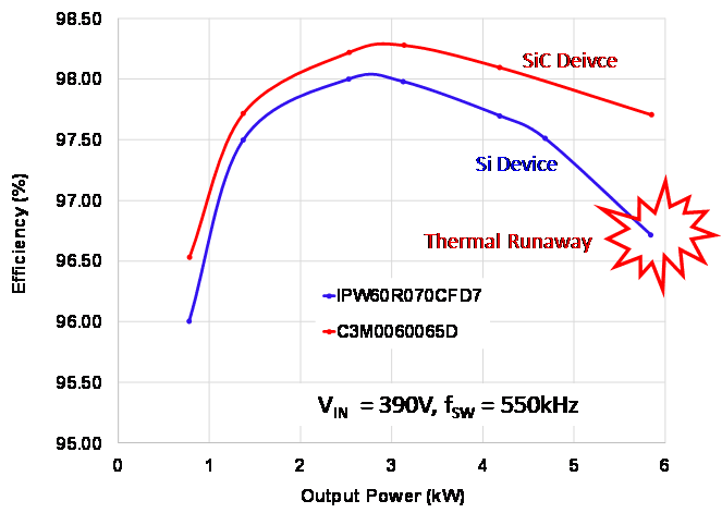
Comparative tests were also done with a Si-based power device (IPW60R70CFD7 from Infineon, 57mΩ600V) for the primary-side switches. Compared to the Si-based MOSFET, SiC-based Wolfspeed part C3M0060065D has much smaller increase in turn-on resistance with increasing junction temperature. Fig. 8 shows the plot of turn-on resistance vs. temperature for these two devices. The normalized turn-on resistance is 1.3 at 150°C for a SiC device, whereas the Si-based device reaches 2.3. Fig. 9 shows the plot of efficiency vs. output power for different power devices. The Si-based MOSFET has 1% lower efficiency at high power and entered thermal runaway with the same heat dissipation because of its significant increase in turn-on resistance with the temperature and higher switching losses.
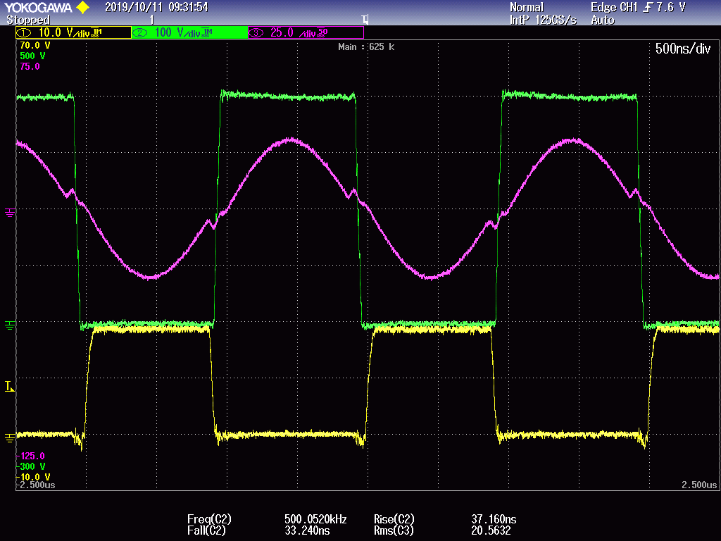
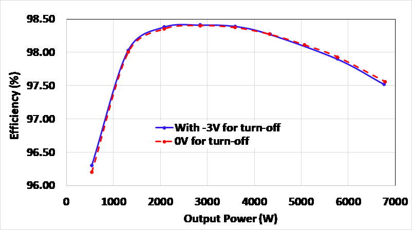
A negative gate-drive voltage (-3V~-4V for C3M006065D) is often recommended for the turn-off of the MOSFETs used in a half-bridge or full-bridge circuit to prevent the false turn-on of the fast switching devices due to the cross-talk resulting from the high dv/dt. However, in an LLC circuit, all the switches are turned on at zero voltage with soft switching, so the dv/dt is much lower and no severe cross-talk is seen. Therefore, the negative voltage for switch turn-off may not be needed to reduce the complexity of the drive circuit and cost. Fig. 10 shows the captured waveforms without the negative voltage for the gate drive. No abnormal gate drive signal is observed and no appreciable efficiency difference is seen from Fig. 11.
Conclusions
An LLC resonant DC/DC converter with SiC MOSFETs and integrated magnetics has been presented and fully tested at 500 kHz – 1.5MHz. It has been found that a careful PCB layout and transformer design is crucial for achieving high conversion efficiency. A peak efficiency over 98% with a power density of 128 W/in3 was obtained. The test efficiency data, along with captured waveforms, have demonstrated the superior performance of silicon carbide (SiC) MOSFETs operated at much higher frequencies than traditional silicon-based devices. Further, tests show that the SiC MOSFETs can operate reliably even without negative drive voltage for the turn-off of power devices in resonant LLC topology thanks to much less severe cross-talk due to ZVS, thus reducing the driving complexity and cost. These wide bandgap devices have offered ever greater opportunity for high efficiency and high power density power conversion in various applications. Future work will incorporate planar magnetics with surface mount power devices to achieve a design of an even higher power density converter.
References
- M. Paolucci, “Improving Power Density and Efficiency in Servers and Telecom,” Power Systems Design, Nov. 2015.
- R. Wang, P. Ning, Z. Wang, et al., “A High-Temperature SiC Three Phase AC-DC Converter Design for > 100 °C Ambient Temperature,” IEEE Trans. Power Electronics, vol. 28, no. 1, pp 55-572, Jan. 2013.
- L. Zhang, S. Guo, X. Li, et al., "Integrated SiC MOSFET Module with Ultralow Parasitic Inductance for Noise Free Ultrahigh Speed Switching," in Wide Bandgap Power Devices and Applications (WiPDA), 2015 IEEE 3rd Workshop, pp.224-229, 2-4 Nov. 2015.
- J. W. Palmour, L. Cheng, V. Pala, et al., “Silicon Carbide Power MOSFETs: Breakthrough Performance from 900 V up to 15 kV,” in Power Semiconductor, pp.79–82, 15–19 June 2014.
- G. Wang, F. Wang, G. Magai, et al., “Performance Comparison of 1200V 100A SiC MOSFET and 1200V 100A Silicon IGBT,” in 2013 IEEE ECCE, pp.3230-3234, 15–19 Sept. 2013.
- B. Lu, W. Liu, Y. Liang, et al., “Optimal Design Methodology for LLC Resonant Converter,” IEEE-APEC Proc., 2006, pp. 533-538.
- W. G. Hurley, E. Gath, and J. G. Breslin, “Optimizing the AC Resistance of Multilayer Transformer Windings with Arbitrary Current Waveforms,” IEEE Transactions on Power Electronics, pp. 369-376, Vol. 15, No. 2, March 2000. 369–76.
- C. R. Sullivan, “Optimal Choice for Number of Strands in a Litz-Wire Transformer Winding,” IEEE Transactions on Power Electronics, pp.283-291, Vol. 14, No. 2, March 19.