Deciphering Data Sheets
Article
How to best decipher the important details contained within data sheets for Wolfspeed’s Silicon Carbide MOSFETs and Schottky Diodes
During the component selection process of hardware design, it’s typical to quickly review datasheets and user guides before committing to a specific chipset. However, depending on the application, it may benefit the designer to explore some of these features in greater detail; unfortunately, it isn’t always straightforward.
This article will focus on how to “decipher” datasheets for Wolfspeed Silicon Carbide (SiC) MOSFETs and Schottky diodes, which have many important details that should not be overlooked. The SiC MOSFET and diode used for these examples are C3M0040120D and C4D30120D, respectively.
Brief overview on pages for SiC components
To save time, it’s best to first focus on the major details, which usually show up on the first page. These details may include the maximum current, voltage rating and RDS(on) values (for MOSFETs), and charge (for SiC diodes). Other details that are good to know right after are the package type and a quick glance at the features in case the application requires specific things like fast switching speed and low reverse recovery (QRR).
The second page will have an overview of electrical characteristics (most of which are for 25˚C ambient temperature). One of the most important parameters in this section are the temperature ratings (case temperature, body diode temperature, and thermal impedance), as the hardware will be dependent on how the device dissipates heat. This should give a good idea of how neighboring electronics and mechanics will be impacted by the junction temperature and what will be needed to cool the part.
Other useful characteristics on this page include on/off timing and delays, along with the total gate charge (MOSFETs), as that will greatly impact its ability to switch in high-frequency applications. When designing a gate driver, VGS,TH will be important, especially when determining the gate drive voltage level.
When looking at maximum ratings, it should be noted that all values hold for 25˚C ambient temperature unless otherwise specified. Also, the test conditions may be different from the operating conditions. Always read the notes that exist for the ratings, as it may affect your design or point you to related figures/plots.
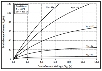
Several of the following pages will include plots that describe performance at specific test conditions. This is important, too, as it will provide a good, reliable picture of how the device will perform given a set of specific conditions that may be similar to your application.
Other information toward the end of the datasheet will include test circuit setup (which is almost always done at double-pulse methodology for MOSFETs) and information on the package size/type with a recommended solder pad layout. Lastly, links for design support may be available toward the bottom, which can take the designer to application notes and other related material that should be reviewed as well. A diode model will be available for SiC Schottky diodes.
Ratings and characteristics of SiC MOSFETs
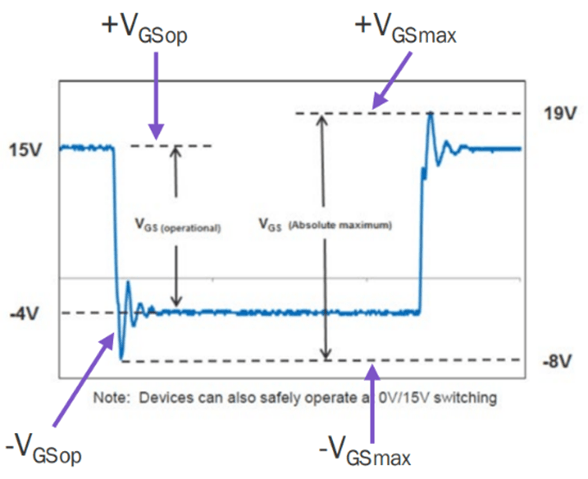
There are three maximum voltage ratings that should be considered for a SiC MOSFET. The first is VDS,MAX, which is the maximum allowable peak value of drain-to-source voltage. Although this will be very high for a SiC component, it’s typically recommended that the application’s max voltage should not exceed 80% to 90% of the max rated voltage to ensure good reliability. VGS,MAX is the max peak value for the gate-to-source voltage during dynamic conditions (switching). This will be important for driving circuitry and should also not exceed more than 80% to 90%. VGS,OP is the max allowable static value of gate-to-source voltage between switching. Figure 1 describes how VGS is related to switching in both a dynamic and static sense.
The continuous drain current can typically be viewed on a corresponding plot (Figure 2) but will be derated with temperature and limited by power dissipation PD, electrical resistance RDS(on), and the bonding wire size. The design’s worst-case continuous RMS current must not exceed this rating. Pulsed drain current corresponds to an energy limitation of the die, and its time duration is limited by case TC, junction TJ,MAX, temperatures and transient thermal resistance (ZTH). A safe operating area (also shown in Figure 2) is determined given the power dissipation, thermal impedance, and pulse-timing characteristics. For both current values, temperature is a function of current, and the designer will need to play a delicate balance between the device’s junction temperature and continuous current conditions.
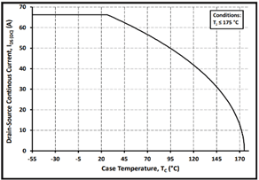
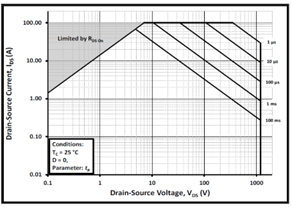
Figure 2: Continuous drain current derating vs. case temperature (left) and safe operating area (right)
In the event of reflow assembly, the part’s max solder temperature should be quickly reviewed and noted that the device can withstand this max temperature for only 10 seconds or less.
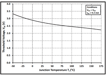
Voltage and current electrical characteristics are related directly to the junction temperature. VGS, for instance, will drop with increased temperature (as shown in Figure 3), introducing risk of false turn-on and decreased overall reliability. RDS(on) also increases with higher junction temperatures and decreases with gate voltage. For SiC components, this relationship of RDS(on), temperature, and gate voltage is much “flatter” than traditional Si MOSFETs, which will give less risk of runaway conditions.
Reviewing switching energy can be important when considering certain configurations of the MOSFETs, such as a half-bridge arrangement. EON and EOFF represent the energy lost during switching transitions and scales linearly with switching frequency. For designs containing SiC Schottky diodes in parallel, less energy will be lost when compared with designs that utilize body diodes only. Additionally, the external gate resistance will have a major impact on these ratings, so it’s important to note that each corresponding plot relates to a specific set of conditions, including gate resistance. The same goes for timing characteristics such as on/off time and delays (see Figure 4). Pay close attention to the test conditions and consider how it may be different for your application.
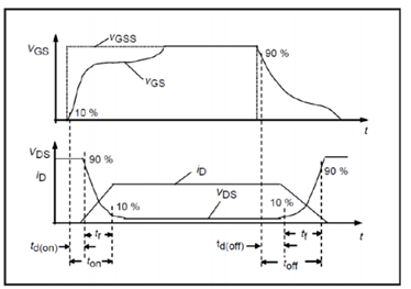
The internal gate resistance (not to be confused with any additional externally applied resistances on the gate pin) will vary widely, between 1 and 10 Ω, based on the device’s construction and internal optimizations. Also, the charge ratings (represented in nanocoulombs, or nC) essentially describe how much the device needs to charge before the channel is completely open and, like before, will depend on the test or operating conditions such as VDS, VGS, and IDS.
The body diode characteristics (shown in Figure 5) describe the behavior of the device when current flows from the source to the drain, such as the body diode’s forward voltage and current. The reverse-recovery charge (QRR) is the total charge that must be swept out of the p-n junction during its reverse-recovery time (tRR), while the peak reverse recovery current relates to how much current flows into the junction. This is important when determining how the device will switch off and to make sure that the body diode can properly manage the residual current (di/dt).
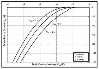
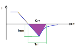
Figure 5: SiC MOSFET body diode characteristics (left) and reverse recovery (right)
The thermal characteristics should be very carefully reviewed, as they will drive heatsink and cooling configurations as well as have a drastic impact on the device’s overall performance. Overdesigning a heatsink can result in unnecessary bulk and cost, while under designing the cooling can limit performance and affect reliability. When pulsed, shorter timing values (duty cycles) will lower these temperature ratings.
Interpreting SiC diode datasheets
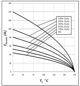
Although a SiC Schottky diode can operate alongside its SiC MOSFET counterpart, its construction is different and has many other characteristics to consider. Because it can have one or two diodes in one package, some sections will rate as “per leg” or “per device,” while other values may represent the package as a whole. And as far as maximum ratings, the voltage is generally provided with some margin from its avalanche value (about 1,600 V to 1,700 V of a 1200V rated device) and includes inductive spikes and other transients that may appear during switching cycles. Though these ratings are much higher than non-SiC components, they are still impacted by junction temperature. The continuous forward current is also directly related to junction current (as seen in a MOSFET), and it derates with increased temperature and duty cycles (see Figure 7). Peak current ratings will vary based on how the diode is driven and the shape of its waveform. IFRM relates to repetitive peak forward current for half-sinewave waveforms, while IFSM is the non-repetitive forward surge current for a single half-sinewave with a specified width. IF,MAX is the rating corresponding to square pulses and generally has the highest of the three peak current ratings.
The power dissipation of each leg/device will vary linearly based on the junction temperature and is ultimately limited by the thermal resistance (R0JC) of the package. Voltage drop will also increase with higher junction temperatures,� and if the datasheet’s plots don’t capture the entire operating range of your application, Wolfspeed can provide PLECS models of each component. The energy for a SiC diode will be represented as I2t and translates to the maximum energy that can be absorbed for a given period of time at a certain case temperature (TC). This is similar to the energy of fuses with finite resistance.
A common failure seen with diodes is when its maximum dV/dt is exceeded and reverse bias is no longer blocked. This characteristic is very dependent on external circuitry and how the device is switched. Bad switching behavior can result in occasional dV/dt transients or ringing over the safety margin, causing device failure and possible damage to other components. SiC allows the diode to provide enough margin (200 V/ns) for most state-of-the-art MOSFETs and IGBTs, but its ruggedness should be considered when designing with other components that may exceed this value.
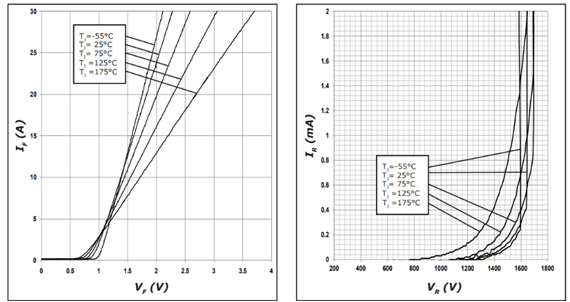
The diode’s forward-voltage drop is directly related to forward current and junction temperature (TJ), as shown in Figure 8. VF will increase with temperature, which helps with paralleling devices. And the reverse current is related to VR and TJ, which will increase with temperature as well. It’s important to note that these values were measured using voltage pulses across the diode to avoid self-heating. The capacitance reported represents a parasitic or differential capacitance that exists between the cathode and anode when the diode is reverse-biased. Though temperature has very limited effect on this capacitance, it’s good to consider how it is impacted through various operating conditions and reverse biases (highest at 0).
The diode’s total capacitive charge describes similar conditions when turned off and residual current decays to 0. The characteristics of this reverse-recovery loss worsens with junction temperature and will generate additional switching losses on the coupled MOSFETs and IGBTs.
Lastly, the diode’s thermal resistance, which is very similar to the thermal resistance for a SiC MOSFET, is the resistance to heat flow from its junction to the case and can be observed on a per-device basis or both devices used in parallel. Again, this is very important for the evaluation of cooling methods and junction temperature during operation. The Z0JC, or transient thermal impedance curves, considers both thermal resistance and thermal capacitance of the materials. Figure 9 demonstrates this characteristic for both the SiC diode and SiC MOSFET.
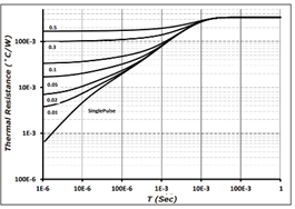
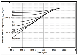
Figure 9: SiC device transient thermal impedance (SiC diode on left, SiC MOSFET on right)
Conclusion
Many ratings and characteristics are presented in SiC datasheets, and it’s beneficial to know how these ratings impact your design. Although SiC provides many advantages over traditional constructions like Si or IGBTs, optimizing things like thermal management, driving topologies, power (voltage/current) conditions, and mechanical interfaces can greatly improve performance and reliability of the design.
Wolfspeed provides several tools and resources, such as PLECS models and detailed reference designs, to help accelerate development.