Design Considerations for Silicon Carbide Power
Article
Silicon carbide (SiC) is a well-established device technology with clear advantages over silicon (Si) technologies, including Si superjunction (SJ) and insulated-gate bipolar transistors (IGBTs), in the 900 V to over 1,200 V high-voltage, high-switching-frequency applications.1 The recent introduction of the 650 V SiC MOSFET products has further broadened SiC use by easily replacing IGBTs, taking a bite out of the Si SJ application share and offering an alternative to gallium nitride (GaN) in the mid-voltage range.
When replacing Si devices with SiC or designing anew with the latter, engineers must consider the different characteristics, capabilities, and advantages of SiC to ensure success. Here is a list of SiC design tips from the power experts at Wolfspeed.
RDS(ON) variance with temperature
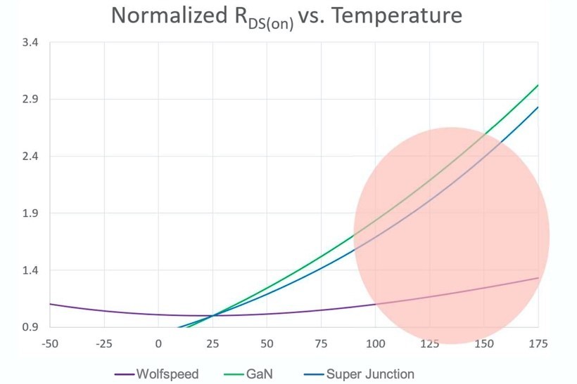
A key advantage of SiC is a low RDS(ON) that changes as little as 1.3× to 1.4× over a wide temperature range, whereas in Si or GaN devices, RDS(ON) may double to triple from that rated at 25°C to the practical junction temperatures in the 120°C to 140°C range (Figure 1). It is therefore important to carefully check the datasheet and specify the correct I2R or conduction loss.
No knee voltage
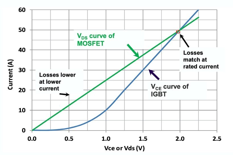
IGBTs are optimized for a thermal design point at the full rated current. Below that point lies the VCE(sat)exponential “knee” voltage curve (Figure 2). SiC MOSFETs’ VDS characteristics are linear, offering lower conduction loss at any point lower than the full rated current.
This is particularly useful to bear in mind when designing EV drivetrains, in which the drive cycle is mostly below the full rated power. When used in parallel, the IGBT VCE(sat) curve exacerbates the problem.
Designers must therefore carefully consider where lies their thermal design point and mission profile.
Effective switching frequency
Effective switching frequency (ESF) is defined as the maximum frequency in a hard-switched application that a device can sustain at the rated IC100 with a 50% square-wave duty cycle without exceeding the device’s specified maximum power dissipation at working voltage. Or:
Where:
The theoretical ESF of a 40 mΩ Wolfspeed SiC MOSFET compared with that of a 40 mΩ Si device is 10× higher. While this offers a glimpse into SiC’s capabilities, cooling, magnetics, and cost put practical limits to switching frequency.
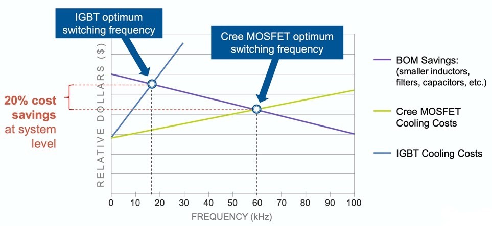
Cooling costs increase, but the passive BoM costs for inductors and capacitors decrease with switching frequency. For IGBTs, the optimum frequency is about 18 kHz, where the cooling and passive BoM savings curves intersect. For SiC MOSFETs, with their lower conduction losses, that sweet spot of cost tradeoffs is at about 60 kHz (Figure 3).
Designers must note that there is a limit to minimizing the inductors, particularly if the system is tied to the grid. And while SiC devices themselves are more expensive than IGBTs, a frequency-optimized design sees a 20% to 25% cost savings at the system level.
Optimizing for applications
The figure of merit (FoM) for a MOSFET is defined by the equation below. The idea behind it is that lower RDS(ON) means lower conduction losses, while lower gate charge, Qg, means lower switching losses. Total losses are minimized if their product, FoM, is minimized.
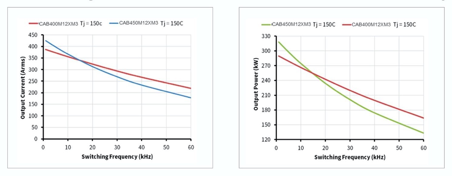
An examination of the output current and output power versus switching frequency characteristics of two of Wolfspeed’s highest-power-density power modules reveals how designers must carefully select the optimal product for their application (Figure 4). The 450 A CAB450M12XM3 module is optimized for very low RDS(ON), but the 400 A CAB400M12XM3 module is optimized for FoM. Over 15 kHz, the 400 A delivers higher current and higher power.
For a motor drive typically operating below 20 kHz, the higher-amperage module is effective, but for solar power inverters switching in the 48 kHz to 60 kHz range, the 400 A module is a better choice.
VDS ruggedness & derating
IGBTs are typically rated at 1.2 kV, with VDS breakdown voltage close to 1.25 kV. Wolfspeed’s SiC MOSFETs, while rated at 1.2 kV, typically have breakdown voltages several hundred volts higher. In aerospace applications, in which designers must derate to account for the effects of cosmic radiation, SiC’s robustness offers an advantage.
Reverse recovery
Designers may not pay as much attention to it when soft-switching or using asymmetric designs, but reverse recovery (Qrr) is important for symmetrical designs, including buck, boost, and totem-pole PFCs. A Wolfspeed 650 V SiC MOSFET would have an 11-nC Qrr for a reverse-recovery time, Trr, of 16 ns compared with a typical 650 V Si MOSFET that has a 13 μC Qrr for a Trr of 725 ns.
Kelvin source pin
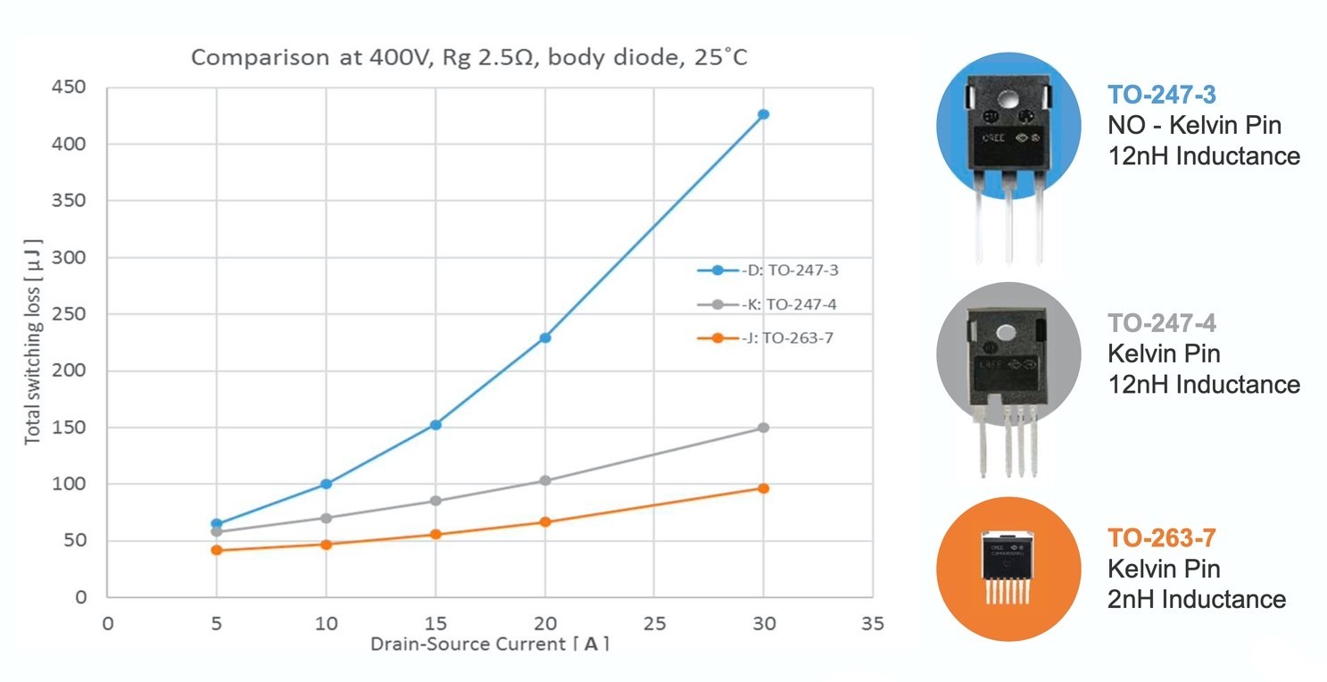
The Kelvin source pin — a Kelvin connection that is as close as possible to the source connection of the MOSFET die — is used to mitigate inductance due to internal bond wires of the MOSFETs. To maintain the high switching frequency advantage of SiC devices, the Kelvin source pin is critical.
The Kelvin source pin also affects switching loss. For instance, at 30 A IDS, the total switching loss in a TO-247-3 SiC MOSFET with no Kelvin pin and 12 nH source inductance is close to 430 μJ (Figure 5). The same product in a TO-247-4 package — with a Kelvin source pin — has merely 150 μJ of switching loss at the same IDS. Moving to a smaller package like the TO-263-7 or the surface-mount D2PAK-7 further reduces the inherent source inductance and the losses.
Gate drive considerations
When driving SiC MOSFETs, designers must remember that a negative gate drive is needed to ensure a hard turnoff, unlike with silicon, in which a positive gate drive is used to turn on the device. Other SiC-specific factors to remember include:
- Faster dV/dt and rated common-mode transient immunity (CMTI) of >100 kV/μs
- Peak continuous working voltage (VIORM) of up to 1.7 kV
- Driving capability that is generally higher power and up to 10 A
- Propagation delays and channel mismatch time typically <10 ns
- Active Miller clamp requirement because of higher switching speeds and a slightly lower threshold at 2 V
- A fast short-circuit protection because of smaller SiC die size (<1.8 μs)
Beyond this, driving SiC devices is much like driving Si-based devices.
Dealing with EMI
Because target switching frequencies are usually higher for SiC devices, and their rise and fall times are much shorter than those of Si products, engineers may be inclined to believe that this would cause greater EMI issues.
However, there is no effect on the low-frequency noise or the differential mode EMI filter size required compared with Si. While there is an effect on the conduction mode noise on the input terminal, it is only in the megahertz range. This high-frequency EMI can be attenuated, just like with Si-based devices, by using high-frequency material and capacitor for EMI suppression.
A wide range of applications
SiC devices are used today in applications ranging from 200 kW UPS, 180 kW EV drivetrains, and 10 kW solar inverters down to 220 W LED SMPS, all designed while keeping in mind a few SiC design considerations and the usual good design principles.
To take a deeper dive into SiC power, watch A Designer’s Guide to Silicon Carbide Power.