Designing for Scalability in High Power Applications
Article
Silicon Carbide (SiC) offers many improvements over traditional silicon (Si) components, spanning a wide range of power levels and applications. With higher operating temperatures, faster switching speeds, increased power density, and higher-voltage/-current capabilities, it can easily be used to replace pre-existing Si-based components and systems, especially when offered in industry-standard footprints such as the WolfPACK product line of power modules. Whether performing a system upgrade or designing a new configuration, SiC provides maximum efficiency and reliability with the lowest losses.
The Wolfspeed SiC product portfolio consists of devices that support all power ranges. Discrete components ranging from 650 V to 1,700 V provide flexibility and low-cost, multi-source solutions, while the WolfPACK family of press-fit, baseplate-less designs offers industry-standard, mid-range power options. And between these WolfPACK modules and the higher-power module solutions, the designer can scale power appropriate to their application and optimize power density, design simplicity, system costs, and reliability.
Designing with paralleled discrete SiC MOSFETs
It’s common to parallel power MOSFETs when scaling current capabilities, but it can sometimes produce issues that aren’t easy to solve. One important thing to consider is the turn on threshold voltage (Vth). Current imbalances can occur when these driving characteristics are different from one MOSFET to the next, which can lead to both higher peak transient currents and static currents.
For instance, Figure 1 shows a plot of current waveforms of two MOSFETs in parallel, one with 2-V Vth and the other with 3-V Vth. Note the differences in overshoot on both turn-on and turn-off. A table also provides the switching energy and loss differences, which, for 1-V difference of turn-on threshold voltage, can lead to significant discrepancies between the two MOSFETs and total power losses.

External gate resistors, which typically range from 1 Ω to 10 Ω, should also be matched as close as possible to prevent timing issues. MOSFETs with lower gate resistances will turn on earlier while also producing higher turn-on transient currents. And MOSFETs with higher gate resistances will turn off slightly later, with more loss during turn-off. Though having individual gate resistors helps with tuneability and optimal per-MOSFET performance, it’s important to understand how these differences can result in loss and timing discrepancies.
Current can also be imbalanced by parasitic inductances, particularly when they are mismatched as well (see Figure 2). These inductances are produced by several things in the design, including PCB layout, unbalanced gate drives, and inherent differences in the MOSFETs themselves. Unbalanced source inductances for 3-lead MOSFETs in parallel can cause circulating current within the gate drive loop, which will cause differences in gate drive voltages. The current of a MOSFET with a lower stray source inductance can ramp up much faster at turn-on and generate much more switching energy. Current can also drop much faster during turn-off, making for higher DC and RMS values and more switching and total power loss.

In addition to loss and timing differences, too many stray inductances on the source (paired with lower gate resistances) can result in gate oscillation, putting the MOSFET into a very unsafe operating area.
Figure 3 demonstrates turn-on and turn-off conditions for two MOSFETs, one with 2-nH source inductance and another with 10-nH source inductance. For this example, the MOSFET with lower common stray source inductance has 19% higher total switching loss and 18% higher total power loss. This is due to the significant di/dt and differences of switching energy. Increasing Rg can help attenuate the oscillation to a safe value; however, it doesn’t necessarily solve the discrepancies of energy loss and timing.

An experiment was performed with a 60-kW DC/DC boost converter using four channels of paralleled SiC MOSFETs (Wolfspeed C3M0075120K with typical 75-mΩ RDS(on)) to demonstrate some of the variances that a specific design or topology might see in hardware differences of two paralleled MOSFETs. In this example, two parts with the highest and lowest threshold voltage were picked out of 60 pieces of sample components. It turned out that one MOSFET (with Vth of 2.666 V and RDS(on) of 67.96 mΩ) carried over 5% more current than the other MOSFET (with Vth of 3.006 V and RDS(on) of 81.82 mΩ). A lower threshold voltage and turn-on resistance result in higher transient currents during turn-on/turn-off and differences in timing, ultimately leading to more power loss.
Another experiment was conducted with a 120-W SEPIC LED driver circuit using two paralleled MOSFETs where it was found that during driving, the MOSFETs became damaged as soon as switching started. Upon investigation, it was found that the PCB layout contained added parasitic inductance at the source of one of the MOSFETs. This was primarily due to the gate drive loop and power source overlapping, as well as an asymmetrical layout. When adding a ferrite bead, it dampened the oscillations and resolved the issue. See Figure 4 for some best practices of laying out PCBs and components to prevent parasitic inductances and sensitive traces equal (and short as possible) with length.
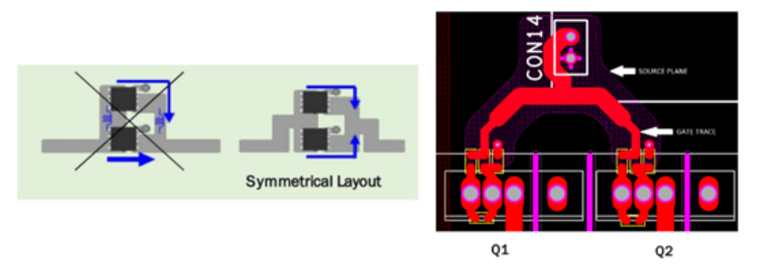
Symmetrical PCB layout is critical for reducing circulating current in the gate loops of paralleled switches, while separating the power loop from the gate loop reduces parasitic source inductance. Also, providing gate dampening components such as ferrite beads helps to prevent gate oscillation. A small Rg (for lower switching losses) with an added ferrite bead is recommended at the gate leg to reduce voltage spikes and ringing on the gate and avoids possible damage to the part. Moreover, adding an external capacitor to the gate and source also helps with reducing the voltage ringing.
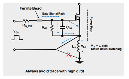
Figure 5 shows a schematic with a ferrite bead added to the gate signal path, as well as the power flow and how stray source inductance slows down switching speed with induced undesired voltage ( = Ls di/dt). It’s important to understand the differences and how they attribute to loss and timing discrepancies when scaling your design with paralleled discrete MOSFETs.
How to scale using Wolfspeed power modules
Wolfspeed power modules containing SiC technology provide the same advantages seen in the SiC discrete portfolio (switching frequency, efficiency, lower losses) but get to really shine in terms of volume, weight, and BOM costs due to the thermal and power density benefits. Up to 40% reduction in losses with 3× higher switching frequency allows up to 37% reduction in passive BOM costs due to the smaller magnetics and reduced cooling requirements for a 200kW active front end (AFE) system. The WolfPACK family provides a scalable, low-cost solution for medium-power applications in a familiar, industry-standard press-fit–pin, baseplate-less footprint. Furthermore, the WolfPACK housing unit allows for flexible configurations, enabling several different kinds of power stages.
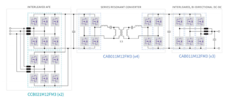
An example of this is a bidirectional electric-vehicle battery charger that can be scaled to the appropriate power level, consisting of three sections (see Figure 6). The first section is an interleaved AFE that eliminates the challenges of paralleled MOSFETs and current ripple minimization. This section can produce 25+ kW per unit (WolfPACK CCB021M12MF3) and be scaled as appropriate. The second section is a series resonant converter that provides high efficiency with 1:1 galvanic isolation and a simple control scheme. With minimal losses and a power delivery of 55+ kW (using the CAB011M12FM3), it provides a scalability for higher-power systems with only needing to regulate the secondary side bus, achieving automatic balancing. The last section consists of an interleaved, bidirectional DC/DC converter. For this setup, boundary conduction mode can be utilized where the current goes slightly below 0 A, which eliminates all turn-on and diode losses to provide an efficiency rate of more than 99%.
When considering some of the higher-power modules, such as the XM3 series, it’s important to select the right module based on switching frequency and max current. The CAB450M12XM3, for instance, offers the highest ampacity/power for applications less than 15 kHz, while the CAB425M12XM3 is suitable for applications more than 15 kHz. And the CAB400M12XM3 offers excellent value and performance for lower-current systems and high-frequency applications.
Like other configurations, it’s best to minimize stray inductance to maximize switching speed and efficiency. Physical layout for SiC devices/modules can have a major impact on the overshoot due to parasitic inductances driving di/dt and induced voltages (that stack on top of the bus voltage). Because SiC enables much faster switching, the overshoot can be much higher than that of Si. So it’s important that best layout practices are followed to lower any added inductance as much as possible.
The DC busbar, for instance, should include planes of laminated copper and equal inductances between each module and capacitors. It must also include a large surface area to help dissipate heat, as well as thicker traces to minimize self-inductance and overlapping planes for added flux cancellation. See Figure 7 for a best practice visual of the strip design (don’t) versus a laminated design (do).

The XM3 inverter offers power scalability within the same module platform and contains offset power tabs that help implement a simple, laminated bus structure. And for cooling, the double-sided Wieland Microcool CP4012D-XP offers a package that has been both physically and thermally optimized for the XM3 module. The cold plate offers balanced coolant flow across all six module positions, each of which have a thermal resistance of 0.008˚C per watt and can support 750-W power dissipation per switch.
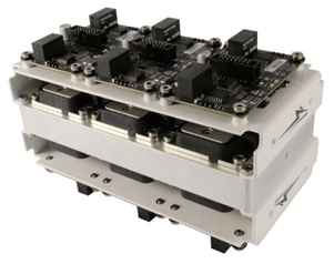
Figure 8 shows six XM3 power modules integrated with the Wieland CP4012D double-sided cold plate (containing high-density pins for optimum heat transfer). The design was meant for a simple, compact system integration and provides a perfect example of a scaled solution utilizing XM3 power modules and optimized thermal management.
For configurations in which there are multiple drivers, such as the dual power core containing XM3 modules, the timing must be well-matched. It’s recommended to have one driver per module to achieve higher drive strength while also giving freedom of timing control.
Another example that utilizes the XM3 power module is a dual inverter power loop (shown in Figure 9). This setup contains a custom DC-link capacitor with integrated laminated bussing for both banks of power modules. It also has dedicated DC input terminals, a low power-loop inductance of 13 nH for bussing and the capacitor, and less than 20-nH total stray inductance, and it operates at more than 98% efficiency. Also shown in the figure is a dual inverter system that has output terminals enabling application flexibility and phase outputs that can be used as a dual inverter or can be paralleled for higher output current.
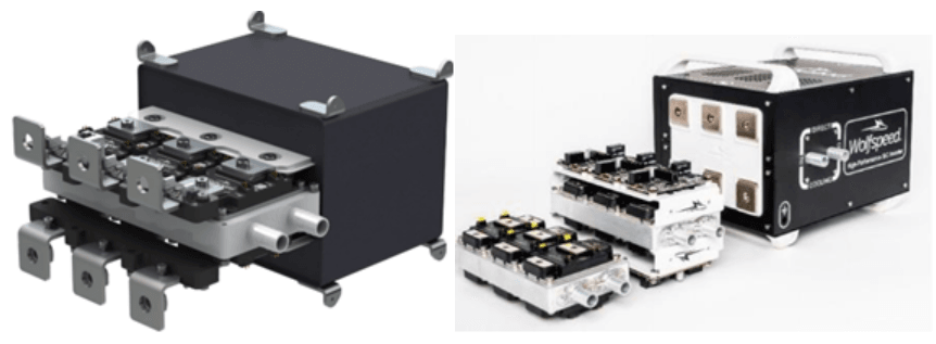
The dual inverter system can provide 375 A per phase as a dual inverter and up to 750 A per phase as a single inverter. When compared with competing technologies (Si IGBTs), the output power capabilities are more than 2× higher (when configured as a dual inverter), while the overall power density is more than 3.6× higher.
Conclusion
To conclude, the power module platforms (Wolfspeed WolfPACK and XM3 modules) provide flexible, scalable solutions for medium- to high-power applications. They maximize power density with a simplified layout and assembly while enabling scalable systems/platforms with interleaved designs, power stage modularity, and simple, symmetrical bussing with timing-matched gate drivers that can easily parallel modules. Power is scalable for both the module and discrete solutions, but it’s important to note that symmetrical layout/design and minimizing stray inductance is critical for maximizing efficiency and achieving current balancing and equal power sharing.