Dynamic Characterization and Measurement Methods
Article
Silicon carbide (SiC) technology has greatly improved power delivery and management across several industries including power supplies, electric-vehicle and home charging, industrial high-power equipment, solar applications, and data centers.
With increased voltage ratings, lower operating temperatures, higher-current capabilities, and better recovery characteristics, SiC has enabled several applications to maximize efficiency and power density while keeping costs at a minimum; however, it’s important to fully characterize these components and their performance in order to take full advantage of SiC technology.
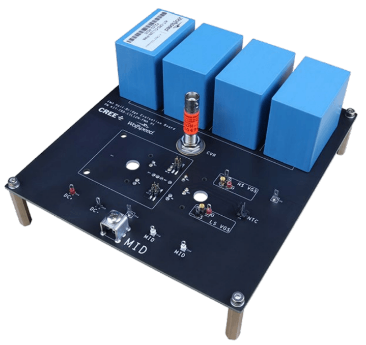
The KIT-CRD-CIL12N-FMA is an evaluation kit that will be discussed in detail in this paper — particularly its dynamic characterization results and the tools required to optimize the switching performance of a SiC power module.
Performing dynamic characterization tests
To measure the four elements of MOSFET dynamic performance, including switching losses, timing, overshoot, and switching speed, the device must be switched and then measured with great accuracy using a clamped inductive load (CIL) test system.
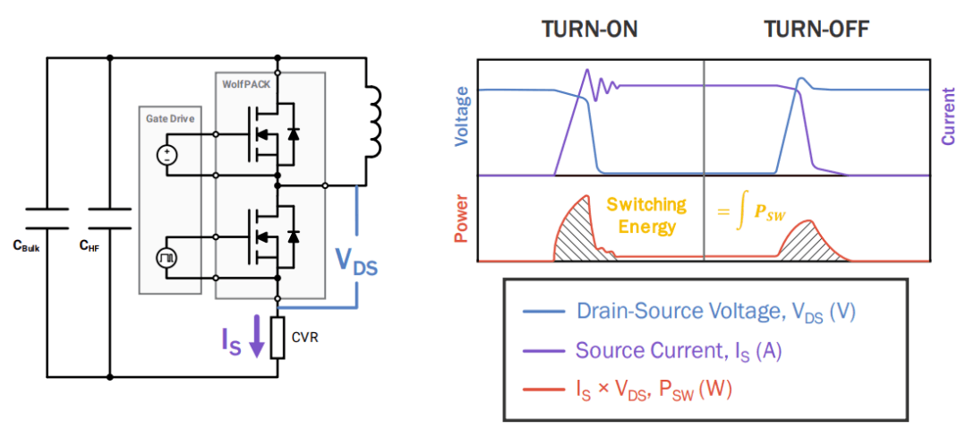
The first part of characterizing the dynamic performance of a MOSFET to measure both voltage and current across the device with a double-pulse test (DPT). By measuring these two waveforms, all information can be extracted and analyzed including losses, timing, overshoot, and switching speed/energy. Figure 2 shows a typical setup in a half-bridge configuration, utilizing a WolfPACK power module and some of the key waveforms and measurements conducted during the test. Following the schematic, it can be observed that when the bottom switch is turned on, the waveforms will show a “turn on” event, displaying peak current/overshoot along with di/dt and dV/dt, Vds. The product of the voltage and current waveforms is the instantaneous power, which, if integrated, will reveal the switching energy lost during transitioning from off to on.
One test that might not be so common during characterization is the diode test with the load inductor across the low-side switch. This helps to characterize the body diode’s performance during switching and demonstrates the reverse recovery behavior.
Best practices for system, PCB, and gate driver layout
Another important thing to measure is the change in MOSFET performance with added gate resistance, which changes the transition speed of the voltage and current (dv/dt and di/dt) as well as raises the switching loss. For an array of MOSFETs configured in parallel, it’s ideal to have an external gate resistor (Rg) ranging from 1 Ω to 10 Ω on the gate of each MOSFET, as this helps to reduce oscillations during switching and prevents the MOSFET from exceeding its maximum voltage rating.
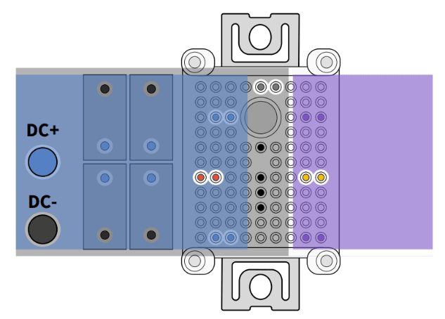
Physical layout for SiC devices can have a major impact on the overshoot due to parasitic inductances driving di/dt and induced voltages (that stack on top of the bus voltage). Because SiC enables much faster switching, the overshoot can be much higher than that of silicon (Si). So, it’s important that best layout practices are followed to lower any added inductance as much as possible. The DC busbar, for instance, should include planes of laminated copper and equal inductances between each module and capacitors. It must also include a large surface area to help dissipate heat, as well as thicker traces to minimize self-inductance and overlapping planes for added flux cancellation as shown in Figure 3.
Additional layers on the bussing PCB help with increased decoupling and flux cancellation, while equal inductance/trace length between the DC-link capacitor and press-fit pins is important as well. On the output of the WolfPACK module, it’s important to include a wide plane to provide maximum current-carrying capacity. Also, never overlap the input and output of these modules, as it can cause added capacitance and increased losses.
There are two main approaches to configuring the gate driver. The first is unipolar, in which, during the “off” state the power MOSFET is held low without a negative bias. The second is bipolar, wherein there are two power sources, one with a negative voltage to help hold the device off during the “off” state and increase overall reliability. Figure 4 shows a comparison of gate driver “on” states with unipolar and bipolar configurations.

For the unipolar configuration, it’s recommended that the Kelvin source plane (signal source plane of the MOSFET) has a large, thick pour right underneath all components with many vias (to maximize current-carrying abilities) to the bypass capacitor and power terminal of the driver IC. Also, placing separate gate resistors per MOSFET has benefits for tuneability and different turn-on/-off speeds. For the bipolar driver, an extra set of capacitors may be needed for the additional negative power rail. Minimizing the high-frequency loop is key to getting the lowest inductance, highest peak current, lowest turn-on loss, and, ultimately, highest performance. Figure 5 shows the ideal layouts for both unipolar and bipolar configurations.

How to measure and characterize parasitic inductance
It can be difficult to measure the parasitic inductance of a SiC MOSFET module due to the extremely low inductance (typically less than 10 nH). The Keysight E4990A impedance analyzer is a great tool for measuring inductance across a range of frequencies (10 kHz to 120 MHz). To interface the equipment to the module, either Keysight-specific probes will be needed, or a custom, rigid PCB fixture with no wires/cables/clips to guarantee the highest level of accuracy.
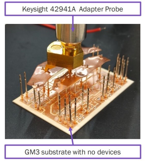
A parasitic inductance comparison was performed with Wolfspeed’s 62-mm WolfPACK module and three competitors using the same setup, and it was found that the Wolfspeed CAB530M12BM3 power module’s parasitic inductance was significantly lower than the competition (11.2 nH versus 15.8–19.2 nH). The GM3 WolfPACK 200-A–rated module was a bit harder to measure for parasitic inductance, but when removing all devices (MOSFETs) and leaving the bonding wire and pins in place (see Figure 6), it provides a very accurate way to calculate the total stray inductance. The raw measurement (with MOSFETs) of the GM3 gives 15.8 nH when run at 10 MHz, while the compensated inductance (just the substrate) measures out at 8.7 nH for 10 MHz. Subtracting the compensated measurement from the raw measurement provides the total stray inductance of the power module, which comes out to 7.1 nH. This demonstrates how important it is to compensate for your fixture and probe as they add a significant amount of inductance measured when using an impedance analyzer.
When looking to optimize the SiC system, the total system inductance must be considered, not just that of the power module or the capacitor. The XM3 provides a great example of this. At 7 nH, it comes in low, but it also enables the bussing design to be low inductance as well (6 nH). This brings the total stray inductance to 13 nH, which is very good for a system as a whole and significantly reduces the amount of overshoot during switching.
Measuring device current and voltage
Measuring the device current and getting accurate results depends greatly on the quality of the probe. At higher frequencies, certain probes will outperform others and reveal more losses and erratic behavior than might be captured with lower-quality probes. For instance, when running a comparison between a T&M Research SSDN-005 probe and a Rogowski coil (PEM CWTUM/3/B), it can be observed that the resistor probe shows more ringing during switching (Figure 7) at frequencies greater than 30 MHz. The figure also shows that the Rogowski coil provides a false sense of switching energy (as much as 20% lower). This is important for characterizing how to switch the MOSFET and knowing what frequency range might introduce more energy losses than what is desired without getting false information.

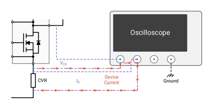
For the VDS measurement, grounding is critical as shown in Figure 8. Two types of probes can be used for these measurements: single-ended and differential. When using the single-ended probe, it’s important to reference your system in a way that prevents multiple grounding points. If measuring directly across VDS without considering the CVR, it can lead to strange behavior due to multiple reference points relative to the oscilloscope. If the CVR is repositioned so that its reference point aligns with the same one for the VDS measurement (providing an inverted signal, which can be adjusted via the oscilloscope), the results are much improved.
Differential probes are another great option. They do well with making low-side measurements but struggle in terms of accuracy with high common-mode rejection ratios, which might come with high-side measurements. The Tektronix TPP0850 is a good single-ended probe, while the Tektronix THDP0200 is a great choice for a differential probe, rated for 200 MHz and 1,500 V.
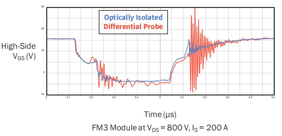
For gate-to-source voltage (VGS), a comparison of an optically isolated probe versus a standard differential probe shows more ringing on the differential probe (see Figure 9). This can alarm designers if they assume that this measured ringing is truly in the system, but in reality it is only a measurement artifact from the differential probe. This false information is due to the differential probe’s low common-mode transient immunity (CMTI) when hit with high dV/dt. Here, the Tektronix IsoVu TIVH05 is the recommended choice for an optically isolated probe.
Post-processing and analysis
Once the information is measured for a variety of components and configurations, there are some things to consider when analyzing and comparing results. It’s best to qualitatively review the switching dynamics of different configurations and find the ideal fit for the application. This process can be quite repetitive on the testing side, but when overlapping waveforms, it helps to reveal the optimal configuration.
When looking specifically at gate driving topologies, Figure 10 demonstrates an example of tests ranging from 1-Ω to 10-Ω external gate resistance, low-/high-side gate voltages, current, and bipolar/unipolar and Miller/non-Miller designs for turn-on conditions of the MOSFET. The plots reveal that for this specific example, the lower gate resistance allows for faster switching but is more aggressive and can cause erratic behavior (at least without Miller clamping). As the gate resistance increases and switching slows, the benefit of the Miller clamp becomes more obvious.
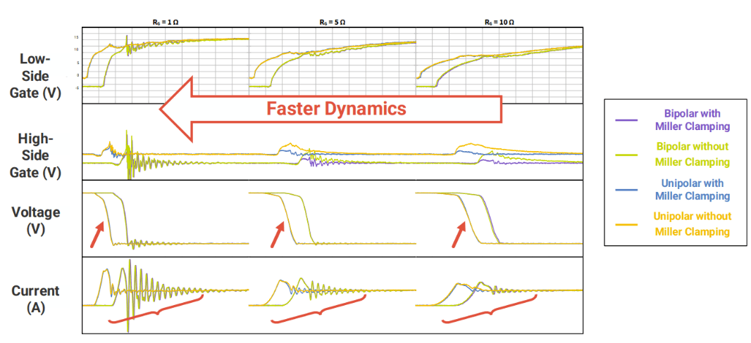
The turn-on conditions consisted of very aggressive switching, including 150˚C virtual junction temperature and 100-A IDS, leading the designer to choose slower switching and thus higher gate resistances for a more stable design. For turn-off conditions, the data is significantly different and less wild with lower gate resistances. If it is acceptable to run the 1-Ω resistor for turn-off conditions, then the design can be optimized for speed (minimizing turn-off delay) and reliability (lower overshoot and ringing) by tuning the two gate resistors accordingly. The same set of plots can also be analyzed for the body diode’s reverse-recovery performance.
When taking it a step further and integrating the voltage and current waveforms, the designer can visualize the performance of switching energy and compare the turn-on and turn-off energy across all cases (see Figure 11). A key takeaway from observing these plots is that bipolar gate driving (15 V/–4 V) with Miller clamping gives the best performance in terms of reliability (no self-turn-on, reduced shoot-through) and switching loss.
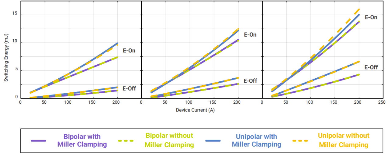
When running the tests and post-processing, it’s important to look at how the MOSFET performs throughout the entire range of junction temperature. For room temperature (25˚C), lower gate resistances might appear to meet the application requirements while maximizing switching speed. However, with higher temperatures, the turn-on/-off characteristics and reverse recovery can change dramatically, increasing loss and instability and taking the MOSFET into an unsafe operating area. These higher temperatures can be tested with a hot plate (or similar) to represent the actual temperature during normal operating conditions.
Conclusion
To conclude, it’s critical to consider several topologies and switching conditions while also utilizing the appropriate equipment that will accurately model the design. Through just four key parameters (switching loss, timing, overshoot, and speed) derived by a few measurement techniques, the ideal configuration can be selected and optimized to take full advantage of SiC’s incredible capabilities.