Gate Drives and Gate Driving with SiC MOSFETs
Article
The use of Silicon Carbide (SiC) MOSFETs has enabled high-efficiency power delivery for a variety of applications, such as electric-vehicle fast charging, power supplies, renewable energy, and grid infrastructure. Although their performance is better than traditional Silicon MOSFETs and insulated-gate bipolar transistors (IGBTs), the driving methods are somewhat different and must be carefully considered during the design process. Here are some example specifications when researching gate drivers for your SiC application:
- A supply voltage range with both positive and negative VGS
- Common-mode transient immunity (CMTI) of more than 100 kV/µs
- Maximum working insulation voltage of up to 1,700 V
- Driving capabilities of up to 10 A
- Propagation delay time and channel mismatch time of less than 10 ns
- Active Miller clamp
- Fast short-circuit protection (SCP) (less than 1.8 µs)
General driving considerations for SiC MOSFETs
Given these specifications, there are a few isolated gate driver technologies to consider. Magnetic coupled drivers are a fairly mature technology but can be a concern in magnetic field applications. Capacitive coupled drivers have great protection from high-voltage stress and improved immunity to external magnetic fields while providing very fast switching with minimal delays. However, the technology is still prone to issues in high-electric–field applications. And the more traditional form of isolation, optical coupling, is very effective and provides great protection against transients and noise but can wear over time with respect to photo gain and LED characteristics.
As system power and frequency increases, so do the gate power requirements. The designer should ensure that the driver has enough drive strength to switch the MOSFET at the desired frequency based on (freq × Qg). Keeping gate driver internal FET RDS(on) low allows for higher current delivery and higher switching speeds, but the total average power specification depends on switching frequency, total gate charge (and any other capacitance placed on the gate), gate voltage swing, and number of parallel SiC MOSFETs or P=(Freq × Qg × Vgs(total) × N). Where P is the average power, Freq is the switching frequency, Qg is the total gate charge, Vgs(total) is the total gate voltage swing and N is the number of devices in parallel.
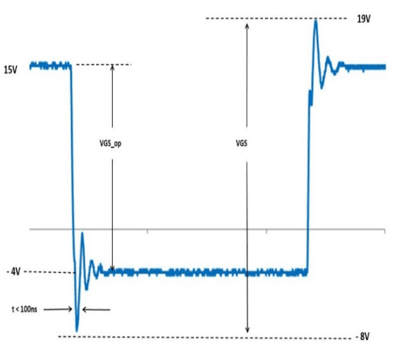
One thing in particular that should be reviewed is the maximum VGS rating, which should allow for ringing and overshoot when switching, as shown in Figure 1. And secondly, the maximum nominal power supply voltage for turn-on/turn-off (15 V, –4 V) should ensure safe operation and long-term reliability. In a practical design with relatively tight feedback control, ±2% of tolerance for turn-on/-off can be achieved, though ±5% is acceptable with multi-winding flyback supplies.

SiC MOSFETs switch much faster than their silicon counterparts, so it is critical that SiC gate drivers be designed to withstand the higher dV/dt (changing rate of drain-source voltage during switching), which can cause ringing and damage to the MOSFET. In hard-switched applications, SiC MOSFETs can generate a dV/dt of more than 150 V/ns, so it is recommended to drive the MOSFET aggressively with smaller values of RG (external gate resistance) and select a driver with a high CMTI rating.
Some PCB layout tips and tricks
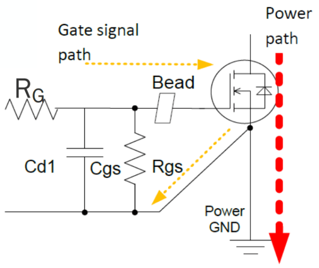
Symmetrical PCB layout is critical for reducing circulating current in the gate loops of paralleled switches. Additionally, separating power loops from gate loops prevents crosstalk, while adding damping effects (such as a gate resistor and ferrite bead) can prevent gate oscillation and reduce voltage spikes and ringing. And a small capacitor (100 pF to 1 nF) placed between the gate and source of the MOSFET provides a low-impedance path for high-frequency noise currents to bypass the gate (see Figure 2).

Here are some additional layout-related items to consider:
- Routing the gate driver and power loops are critical; keep them separate from each other.
- Parasitic inductance and capacitance can have a dramatic effect on performance and switching behavior due to high di/dt and dV/dt in SiC systems. Some tips on reducing parasitic effects:
- Capacitance on the switching node increases losses.
- Inductance in the bus loop increases voltage overshoot at turn-off.
- Inductance and capacitance in the gate circuit reduces switching speed and control of the gate voltage.
- Differences in inductance or capacitance seen by parallel devices will result in imbalances.
Paralleling MOSFETs can increase power in a design
Paralleling MOSFETs enables high-power designs (such as an interleaved boost converter) and can be done at multiple levels. When implementing a driver for parallel MOSFETs, their gates should not be tied directly together, and instead, gate resistance should be applied separately to each gate. Also, any asymmetry in the power path’s layout can generate a voltage imbalance between the sources during switching transitions. Stray inductance (that may vary between 1 and 15 nH) can also generate unbalanced, oscillating voltages, but increasing the gate resistance and adding ferrite beads can add damping effects to help reduce oscillations and switching loss. Also, adding a 1-Ω resistor to the source of each SiC MOSFET can dramatically reduce any high peak currents that may flow, as well as act as automatic feedback to the VGS, helping to improve dynamic sharing (see Figure 3).

Some of the same rules apply when implementing modules. It’s important to connect the switching nodes to the load symmetrically and ensure that impedance from each module to the DC bus is matched. When paralleling modules, the designer can choose between a shared gate driver and separate gate drivers. Sharing the gate drivers helps eliminate timing mismatches between different drivers, but the gate driver boards can be difficult to lay out, especially for more than two parallel modules. Separating the gate drivers requires a low part-to-part timing skew.
Figure 4 shows some layout examples of laying out driver boards for parallel MOSFETs.

Negative driving voltages allow for safer operation and improved noise immunity
Normally, MOSFETs are fully turned off at 0 V. Adding a negative gate bias improves noise immunity and avoids false turn-on in half-bridge configurations, but for single-ended power converters such as flyback, boost, or buck converters, using a 0-V turn-off voltage is acceptable. When using a totem-pole topology, high dV/dt and di/dt often results in crosstalk and can generate ringing and voltage spikes at the gate, so a negative-voltage (such as –4 V) steady-state setting will give enough margin for spikes not over –8 V. And if the PCB layout has been optimized, the negative gate bias can be closer to –3 V or –2 V (lowering this bias in turn lowers the forward voltage of the body diode), as long as there is no false turn-on.
Implementing a positive and negative gate drive voltage solution can be done in a number of ways. For example, a dedicated 15-V/–3-V integrated power supply component can help reduce part count, while designing a discrete arrangement with an 18-V output and then generating –3 V via a resistor and Zener diode can provide more flexibility. Another option is to use a gate driver IC with a built-in DC/DC controller, such as the Si8281. And lastly, you can customize your own complete solution by using a push-pull circuit, such as the TIDA-01605 from Texas Instruments (see Figure 5).

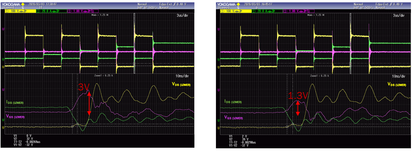
Adding an active Miller clamp to a totem-pole half-bridge design can greatly reduce crosstalk by activating at 2 V when the MOSFET is turned off while bypassing RGext, reducing the parasitic turn-on bump (see Figure 6 for comparison using C3M0060065J at 400 VDC). In order for this to work, the driver must be very close to the MOSFET so that stray inductance is minimized.

Other recommended tests and tweaks
Protecting your design from overcurrent (or short-circuit) is a must, and most designers prefer the “de-sat” approach over a current shunt. Although the current-shunt topology provides a fairly accurate trip level, it dissipates a lot of power while requiring significant PCB space. Thus, the current shunt is recommended for lower-power applications that need accurate trip currents to protect their respective loads. The de-sat mechanism works well for SiC devices, as it introduces no additional loss and can be used for higher-power loads/modules. However, the de-sat approach only trips on Vds, not the device’s actual current, which results in a wider variation of trip level. Figure 7 demonstrates the difference between a shunt-based and a drain-voltage–based SCP design for a SiC MOSFET.

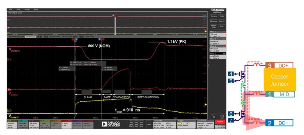
Designing for SCP is important, but fine-tuning the cutoff parameters can be tricky. The designer must adequately protect the SiC MOSFET while not allowing for any false trips. The “de-sat” voltage level must be selected based on the MOSFET’s RDS(on), along with the worst-case conditions, including high temperature, peak currents, and the max value of RDS(on). The de-sat detection time should be selected based on switching transition time and noise immunity, and again, consider the worst-case conditions, such as low current/slow switching and high current/ringing. To ensure protection with no detrimental effects to the SiC die, Wolfspeed recommends the following conservative recommendations: 250–500 ns of detection time after turn-on, 400–1,500 ns of soft-shutdown duration after detection, and a short-circuit duration of less than 1–1.5 µs.
In most SiC modules, short-circuit faults must be detected when the device is still ringing (less than 1 ms) and hasn’t saturated. Unlike an IGBT, the fault on a SiC device may have to be detected before the short-circuit current reaches a peak. A destructive test can be performed to test this feature, such as the example test shown in Figure 8. This test involved an ADuM4177 gate driver and CAB450M12XM3 SiC module (rated for 1,200 V/450 A). The fault was detected within 550 ns and shut down in the following 360 ns.

Conclusion
To conclude, SiC technology enables high-efficiency and high-power–density systems but must be driven with several strategies in mind. The gate driver must have a sufficient drive capability to reduce switching losses and operate at high-enough switching frequencies, and it must have high CMTI, minimal parasitics, and an optimized de-sat detection and soft-shutdown feature. When laying out a PCB, aim for symmetry and short traces for sensitive signals to prevent crosstalk, use passive components such as capacitors and ferrites to help with noise rejection, implement individual gate resistors to keep things balanced, and keep things cooled/thermally managed in a uniform manner.
Wolfspeed offers several design support tools, such as evaluation kits for all discrete packages, gate driver reference designs, general reference designs, and demo platforms for MOSFETs and power modules, and online/offline simulation tools and models.