High-Performance 300 kW 3-Phase SiC Inverter Based on Next Generation Modular SiC Power Modules
Article
Abstract
Wolfspeed presents a new high-performance, low-cost, compact 3-phase inverter based on next generation power modules which are specifically optimized to fully utilize Wolfspeed’s third generation of Silicon Carbide (SiC) MOSFETs. The inverter was designed with a holistic approach with careful consideration of module specifications, busbar technology, DC link capacitors, and a high-performance thermal stackup. Parasitic elements of all critical components including the module, busbar, and capacitors are validated to ensure the lowest overall stray inductance. The XM3 module is 60% by volume smaller than equivalent power rated modules which enables the inverter to achieve a power density of 32 kW/L. The unit is tested under application conditions with an 800 V DC bus and 360 A phase current.
This paper was first published at the PCIM Europe Conference in 2019.
1 Module Design Considerations
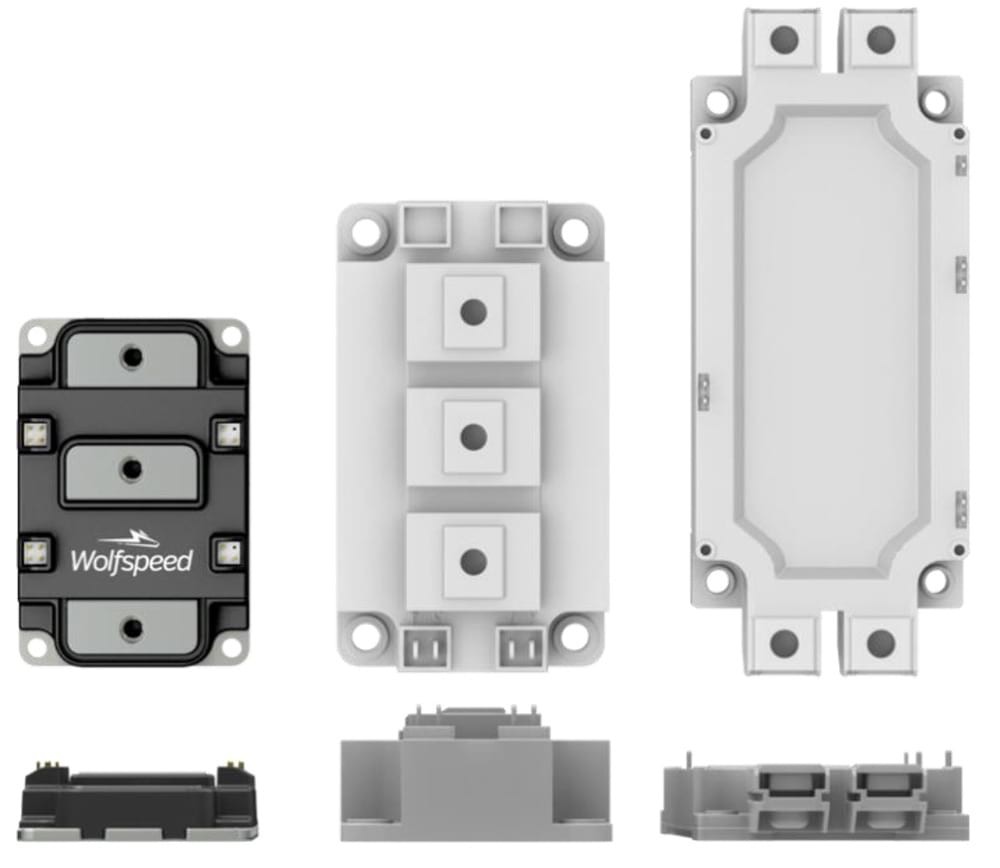
Conventional power packages are an effective and well accepted industrial solution for state of the art silicon (Si) IGBTs. However, they often struggle to take full advantage of what Silicon Carbide based technology offers. Their footprints and internal layouts were originally designed for Si devices, which typically have a single or small number of paralleled large devices with signal networks following long paths. The bipolar nature of IGBTs limit the switching speeds such that the mentioned design trade-off is acceptable. Modifying these packages to accommodate SiC is possible but not without compromise.
To fully utilize the high-performance attributes of Silicon Carbide devices, a technology centric design is required of the power module. This power module design overcomes the shortcomings of existing module designs. SiC centric designs must enable arranging multiple smaller die in parallel such that they share dynamic current evenly and optimize the signal network with short path parallel planes such that the SiC die switch evenly even under high speeds. However, the product must strike a practical balance between performance, cost, and manufacturability.
To meet these needs, Wolfspeed has developed a next generation module that has been highly optimized to achieve the maximum performance out of all sizes of commercially available 650–1700 V Wolfspeed Generation 3 SiC MOSFETs. It offers the capability to carry high currents (300 to >600 A) in a small footprint (53 x 80 mm) with a terminal arrangement that allows for straightforward bussing and interconnection. A lowinductance, evenly matched layout results in high quality switching events, minimizing oscillations internal and external to the module. The module has a stray inductance of 6.7 nH and approximately 60% the area of a 62 mm module as can be seen in Fig. 1.
1.1 Terminal Layout
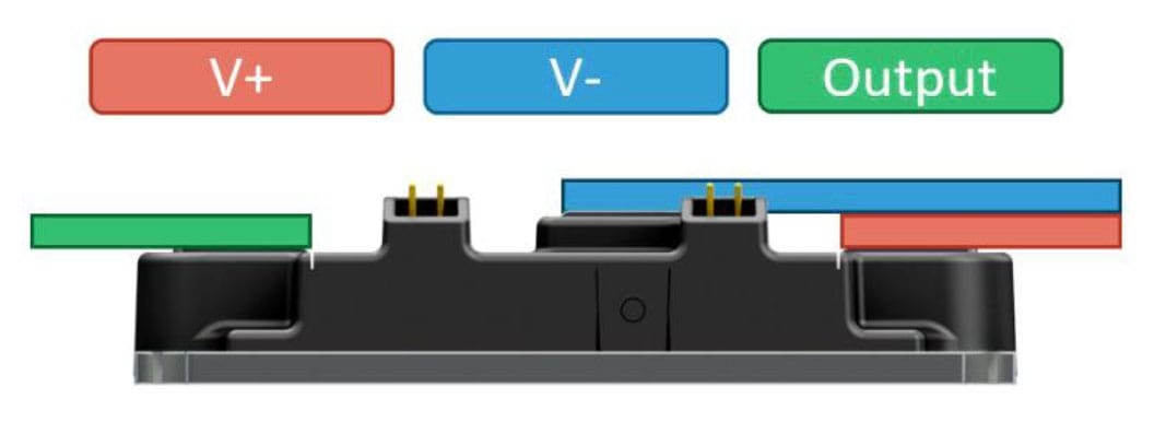
The current loops have been designed such that they are wide, low profile, and evenly distributed between the devices so that they each have equivalent impedances across a switch position. The power terminals are vertically offset as shown in Fig. 2 such that the bus bars between the DC link capacitors and the module can be laminated all the way up to the module without requiring bends, coining, standoffs, or complex isolation. Ultimately this achieves a low-inductance throughout the entire power loop from the DC link capacitors to the SiC devices. A XM3 module without devices was connected to a Keysight E4990A Impedance Analyzer to extract the parasitic inductance of the package. The power loop inductance from V+ to V- is 6.7 nH measured at 10 MHz
1.2 Inductive Switching Loss
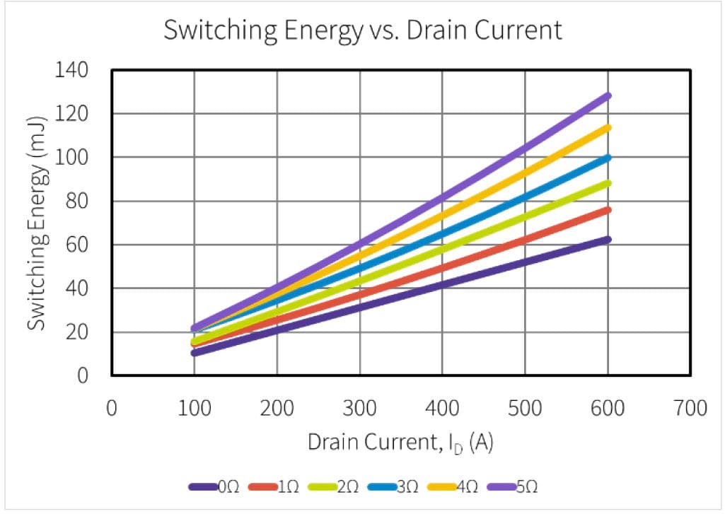
The XM3 utilizes internal gate resistors with a short gate signal loop and wide, low inductance paths to guarantee that all the paralleled devices remain stable during high switching speeds. The modules can be safely used with zero external gate resistors when a low-inductance bus structure and low-inductance capacitors are utilized as shown in Fig. 9 and Fig. 10. This removes the burden from the designer when sizing external gate resistors to ensure they do not trigger any unwanted characteristics and maintain RBSOA. At 800 V and 400 A the switching loss, including reverse recovery losses, is 42 mJ for RGext of 0 Ω. Additional external gate resistance can be utilized if desired. The switching loss for various gate resistors is shown in Fig. 3.
2 Inverter Design Considerations
To take advantage of the low-inductance power module the remaining power components of the inverter’s DC side must be designed to minimize stray inductance. Lower power loop inductance results in lower peak overshoot voltages seen by the switches as well as reduction in ringing and oscillation. A complete low-inductance structure therefore enables faster turn-on and turn-off times and thereby lower switching losses.
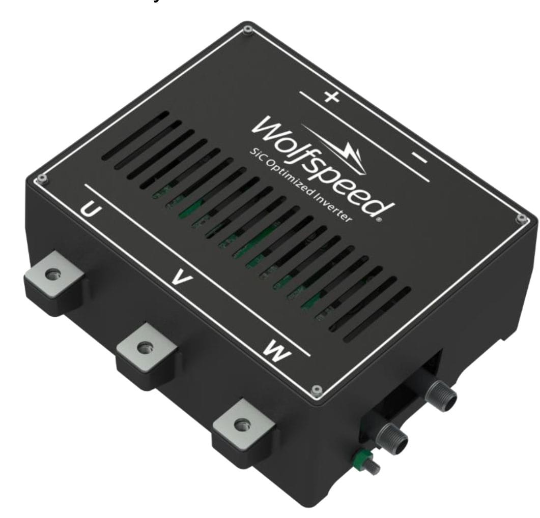
The design philosophy for the inverter directly follows the design philosophy utilized in the module: maximize performance through highampacity, low-inductance designs while minimizing cost and complexity. To achieve this, 5 key parameters were considered. First, due to the high current density achieved through SiC devices and compact module size, a high-performance thermal stackup must be implemented to maximize heat transfer. Second, the stray inductance introduced by the busbar structure should be minimized through the use of low-inductance, overlapping planar structures. Third, to close the high-frequency switching loop effectively, lowinductance and high ripple rating capacitors must be utilized. Fourth, optimal device control with high-speed protections and high-noise immunity must be utilized in the gate driver to effectively switch the devices and provide maximum survivability under fault conditions. Finally, the entire structure’s cost should be minimized and the entire stackup should be engineered to minimize complexity for assembly and manufacturing. The inverter measures 279 mm by 291 mm by 155 mm for a total volume of 9.3 L and a power density of 32.25 kW/L. This design offers an improvement over Wolfspeed’s previous 250 kW, 1.2 kV 3- phase inverter of ~65% reduction in volume and ~340% increase in power density [1].
2.1 Thermal Stackup
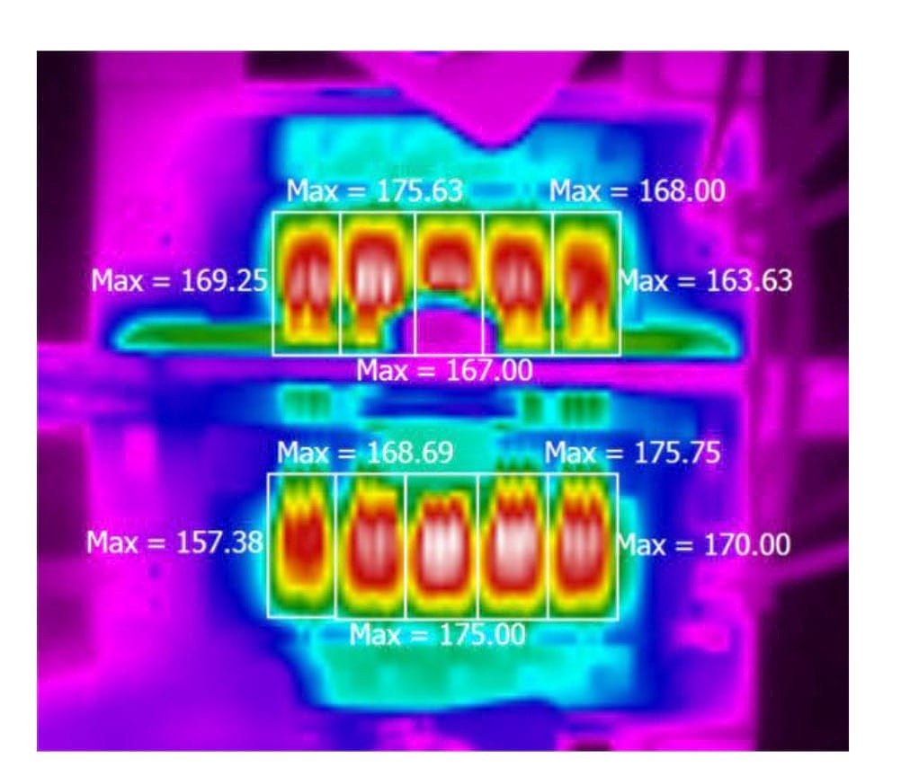
Due to the high current density of Silicon Carbide power devices the thermal performance of the module, TIM, and cold plate is critical to reduce size and weight. A custom micro deformation liquid cooled cold plate developed by Wolverine™ has been utilized to meet the high-performance thermal requirements of the XM3 package. Thermal tests of the XAB450M12XM3 mounted onto this cold plate with 25°C coolant can dissipate 670 W per position for a total of 1340 W with the devices at the maximum junction temperature of 175°C. The thermal image in Fig. 5 shows little variation between the die. With 670 W per position, the inverter can process 360 ARMS with the XAB450M12XM3 operating at 20 kHz switching frequency and 800 V bus.
2.2 Busbar Structure
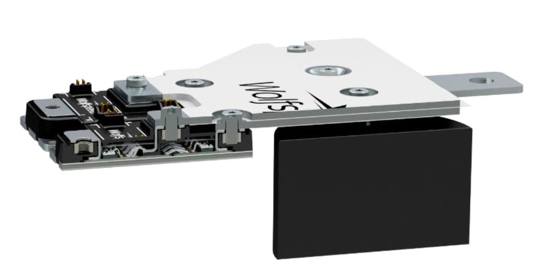
The vertical offset of the module’s power terminals allows the busbar design to remain simple and cost-effective while maintaining a low power loop inductance. A low-inductance busbar is utilized to interconnect the DC-link capacitors (located under the busbar) to the power modules. Again, the offset power module terminals enable the busbar assembly to have no bends, which reduces cost and maximizes overlap. The capacitors are affixed as close as possible to minimize the total loop area. As can be seen in Fig. 6 the busbars consist of one flat plate connecting V+ terminals of the modules and capacitors followed by an insulator and then a second flat plate connecting to the raised V- terminals of the modules and the capacitors with coining or spacer for the capacitor terminal. The structure is simple enough that it can be made with minimal fabrication which reduces the cost and lead-time. Optimized orientation for the capacitors was determined by measuring the inductance of three prototypes of the bussing geometry fabricated as two-layer PCBs. Between each prototype the capacitor terminals were rotated vertically, horizontally, and diagonally at 45 degrees. The horizontal orientation offered the lowest relative inductance with capacitors installed and is the orientation used for the laminated bussing. Iterative design process with small-signal parasitic extraction made it possible to test multiple configurations to find the optimized bussing geometry.
2.3 Capacitor Selection
There are three key parameters when selecting DC link capacitors; peak voltage rating, ripple current rating, and equivalent series inductance (ESL). The voltage rating must exceed the DC bus voltage plus overhead for peak overshoot voltage during turn-off. For the 900 V bus the minimum capacitor voltage rating is chosen to be 1100 V. The ripple current requirements are load current dependent and will be shared between paralleled capacitors. The capacitors are included in the total power loop and will contribute to the total inductance. Low-inductance capacitors are necessary to take advantage of the switching performance improvement provided by the XM3 package. The CX100U1100D51 by Fischer & Tausche™ fulfill these requirements with 100 A current rating and 10.5 nH ESL per capacitors. The high current rating of this capacitor allowed for the use of three in parallel for a total ripple current rating of 300 A and capacitor inductance of 3.5 nH
2.4 Control System
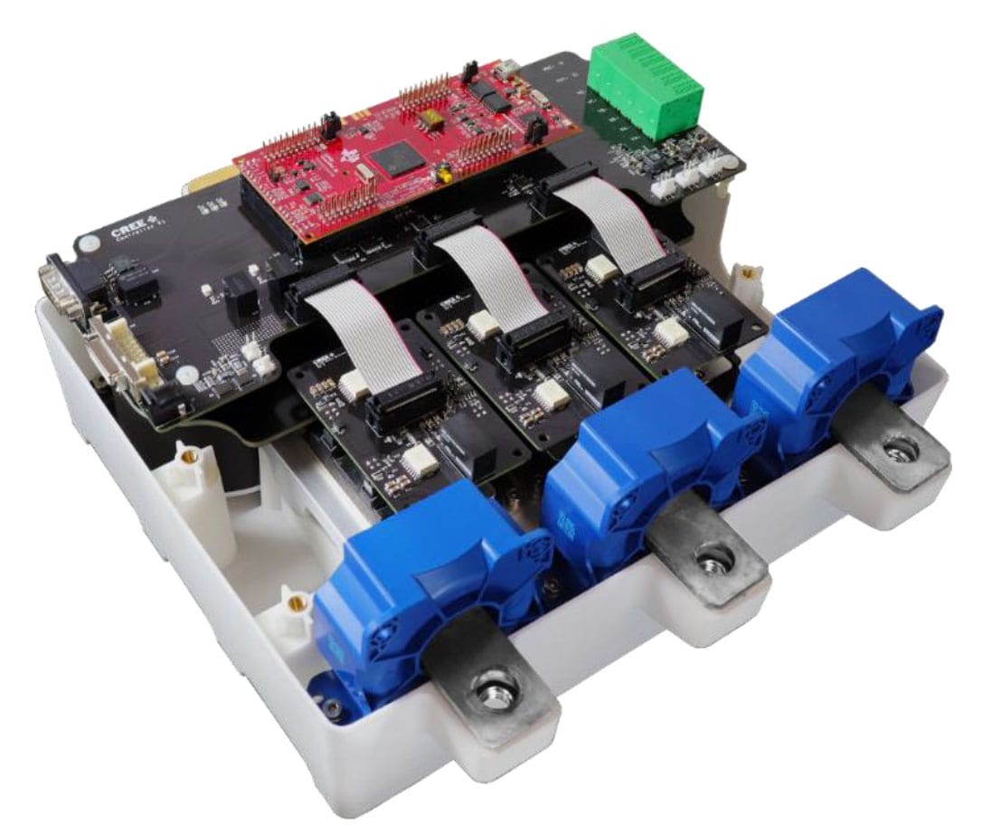
This inverter reference design includes sensors, interface, power supplies, and controller necessary for a complete motor-drive or inverter system. Three current sensors are included at the output terminals and differential, high-voltage measurements are provided for the DC bus and three external connections. Isolated gate drivers are connected via ribbon cable to the controller PCB which provides power, differential signals, as well as control signals. External high voltage sense connections are made on a separate side of the enclosure from the low voltage external connections for I/O and power. An external, protected +12 V DC power jack powers the low voltage circuitry including gate drivers, controller, and current sensors. A powerful floating-point DSP is used to run the control-loop for the inverter as well as handle I/O.
2.4.1 Gate Driver
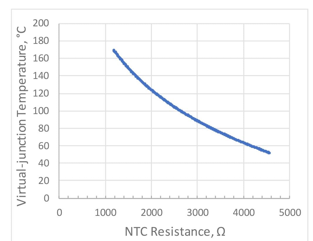
A footprint matching gate driver for the XM3 platform is used to drive each of the three power modules. The gate driver has been optimized for Wolfspeed’s C3M devices to extract the maximum performance from the modules. +15 V / -4 V voltage rails are used for the output stage of the driver to match the recommended VGS rating for C3M devices. Murata™ MGJ2D121505SC provide 2 W for each channel with an isolation voltage of 5.2 kV with only 2.9 pF of isolation capacitance. Protection features of the gate drivers include programable over-current detection with softshutdown, under-voltage lockout, and anti-overlap of PWM inputs. The over-current detection circuit forward biases a high-voltage blocking diode connected to the drain terminal during the on-time and latches a fault signal if the voltage exceeds to a tunable threshold. Differential signaling is used on all input PWM, fault, and temperature outputs. Improved common-mode transient immunity of RS-422 differential transceivers eliminates signal corruption associated with high edge rates that SiC switches can generate. Additionally, the temperature sensor built into the power module is sensed and fed back to the controller via an isolated PWM signal. The temperature sensor is positioned as close as possible to the power devices while remaining electrically isolated from them and therefore provides an approximate baseplate temperature. The NTC resistance is correlated to the virtual-junction temperature for this inverter as shown in Fig. 8.
2.4.2 Current Sensors
The output current sensors are LEM™ LF 510-S, 500 A, closed-loop current transducers. This part has an insulation voltage rating of 1500 V between primary and secondary circuits. A current output signal is preferred for better immunity against electrical noise injected into the wiring between the sensor and the controller. Closed-loop transducers have higher accuracy and lower temperature drift compared to open-loop transducers. The output busbar for each phase passes through the aperture of one of the current sensors, and the output signal is fed back to the controller. The controller features a DC/DC converter to provide the bipolar ±15 V power required for the sensors. Provisions for a fourth current sensor are available on the controller board for an external sensor to measure an additional current.
2.4.3 Controller Board
The DSP is a TI™ Delfino™ TMS320F28379D with dual 32-bit cores running at 200 MHz with built-in CAN modules, position encoder modules, and 12- bit ADCs which make it ideally suited for closedloop real-time control. Dual floating-point cores allow for the separation of fast control-loop from slower application code onto separate parallel CPUs. The built-in peripherals of the Delfino series are targeted at real-time embedded control system applications such as including two CAN modules for communication, two position encoder interfaces for motor drives, four independent ADCs with 12-bit resolution and 24 external inputs, and 24 advanced PWM outputs. The controller board has filtering and signal conditioning circuits for all the analog feedback signals in the system. This includes four current sensor signals from LEMs, three module temperature sensors, and a temperature sensor controller board. The four voltage measurements are brought to the controller as high voltage and must be accurately stepped down to a safe voltage for the ADC. This is done for increased noise immunity as noise can easily corrupt a low voltage signal such as commonly used 0-5 V signals. An isolated CAN interface with industry standard DE9 connector is provided for communication with a host system. The controller is powered by the previously mentioned +12 V power jack.
2.5 Enclosure Design
The inverter utilizes a low-cost, highly-integrated plastic case with built in mounting points for all components. This approach eliminates the need for spacers and stand-offs and minimizes insulation coordination concerns. The custom plastic structure allows the inverter to be compact and have reduced weight by eliminating the outer sheet metal case. The top half of the case has mounting provisions for the gate drivers and the control board with opening for the external connectors. A sheet metal lid attaches to the top half of the case and has slots cutouts for ventilation
3 Experimental Results
To validate the high-performance nature of the system, the components must be evaluated in both the frequency and time domains. Small-signal parasitic extraction enables an accurate measurement of parasitic elements which can be utilized in an iterative design process to minimize stray inductance as was shown with the bussing. The impedance from the module’s perspective is measured to be 5.3 nH (combination of bus bar inductance and DC-link capacitor inductance). The 5.3 nH of the busbar and DC-link capacitors combined with the 6.7 nH of the module create a total loop inductance of 12 nH. This value is already much lower than the stray inductance of many legacy power modules packages by themselves [2],[3]. Due to the lower inductance, the inverter can switch much faster without violating the breakdown voltage rating of the devices from turn-off overshoot
3.1 Inverter Switching Results
The waveforms in Fig. 9 and Fig. 10 show a double pulse test of the module, busbar, and DC-link capacitors. At 840 V and 620 A, minimal voltage overshoot is shown (approximately 240 V) with minimal ringing. Measurements were taken using a high voltage differential probe for VDS, a 600 A, PEM™ Rogowski coil with 23 MHz bandwidth, and 500 MHz bandwidth Tektronix™ IsoVu™ optically isolated voltage probes for both high side and low side VGS.
3.1.1 Turn-On and Turn-Off Waveforms
The waveforms shown in Fig. 9 are from an inductive load test of one of the positions of the inverter with a 14 µH load. These results show the quality of switching waveforms possible with the XAB450M12XM3 and RGext of 0 Ω. The peak overshoot voltage during the MOSFET turn-off at 840 V is 1080 V with a voltage slope of 19 V/ns with low ringing. The turn-on current at 620 A showed an overshoot of 710 A and a current slope Fig. 10 demonstrates the body diode dynamic characteristics at 840 V and 600 A with RGext of 0 Ω. The maximum voltage and current edge rates during turn-off are 17 V/ns and 15 A/ns respectively. The peak voltage overshoot observed during turn-on (reverse recovery event) is 954 V. Minimal reverse recovery current and loss is observed with the built-in body diode as previously shown [4]. Both the MOSFET and body diode switching waveforms demonstrate that the inverter can achieve very low switching loss with very little ringing even with minimal gate resistance
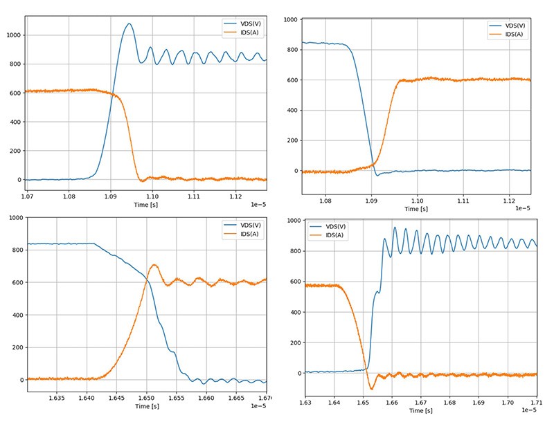
Figure 10 (right): Switching waveforms for upper switch during turn-off (top) and turn-on (bottom).
3.1.2 Over-Current Fault Operation
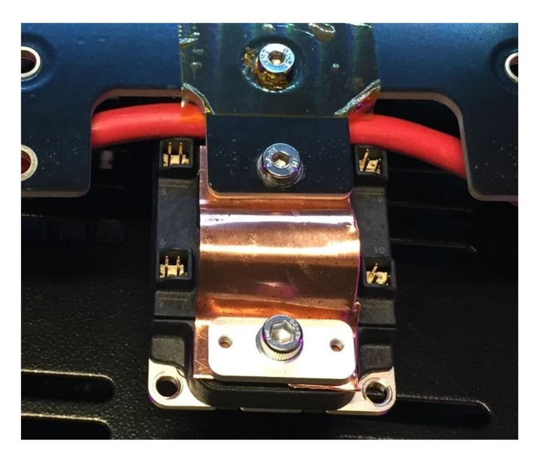
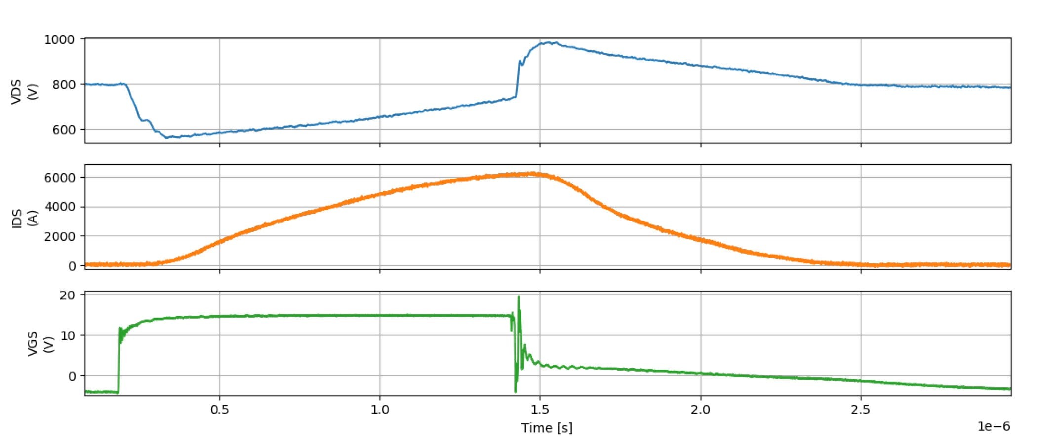
Over-current fault protection was verified by shorting the lower switching position of the XM3 power module with a short copper strip from the output terminal to the V- terminal. This configuration, which can be seen in Fig. 11, simulates a load short and in the case of the copper strip a very low-inductance load short. The soft-shutdown feature of the gate driver pulls the gate down to the negative rail through a separate tunable resistor when an over-current event is detected. The soft-shutdown resistor is set to be slower than the standard gate resistor to limit excessively high voltage overshoot when turning off high currents. Fig. 12 demonstrates a typical performance of the over-current protection. The length of the current pulse is set by the minimum blanking time of the detection circuit which for this gate driver is approximately 1.2 µs. The peak current reached during the test is 6.2 kA while the maximum drain voltage during turn-off is only 985 V. The length of the current pulse is approximately 2 µs, which is below the short circuit withstand time of the devices [5]. These results demonstrate that simple desat style protections can be utilized with SiC by simple optimization of the blanking time and shut-off method.
3.2 Single Phase Power Testing
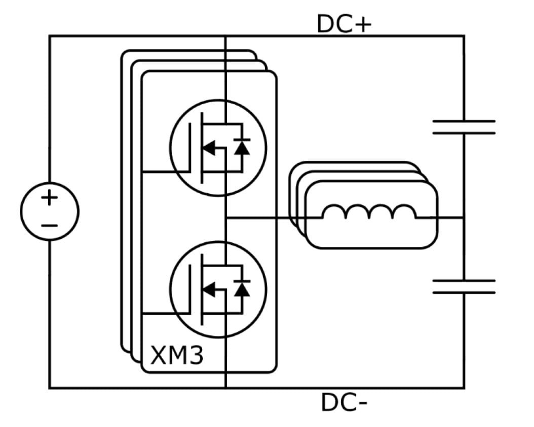
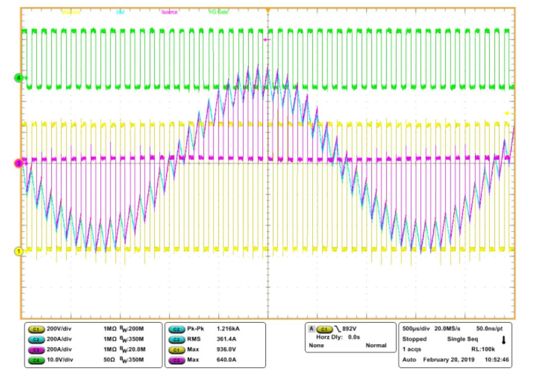
The power testing of the inverter stack was first demonstrated with a single-phase recirculating power test bench. The load inductor is connected between one of the output terminals of the inverter and the midpoint of a large capacitor bank. A DC power supply is used to charge the capacitor bank and to supply the losses of the system. Energy is transferred from one half of the capacitors to the other half through the inductor during each switching cycle. The direction of energy transfer reverses over one cycle of the fundamental frequency. The power factor is unity from the perspective of the inverter because the current and voltage is always in phase. The schematic for this test setup is shown in Fig. 13. The load current and the upper switch position drain current are monitored along with the midpoint voltage and the upper switch’s gate voltage. The bus is set to 800 V and the modulation factor is increased until the load current reached 360 ARMS with a calculated loss of 930 W for the module. The captured waveform for this test is shown in Fig. 14.
3.3 3-Phase Power Testing
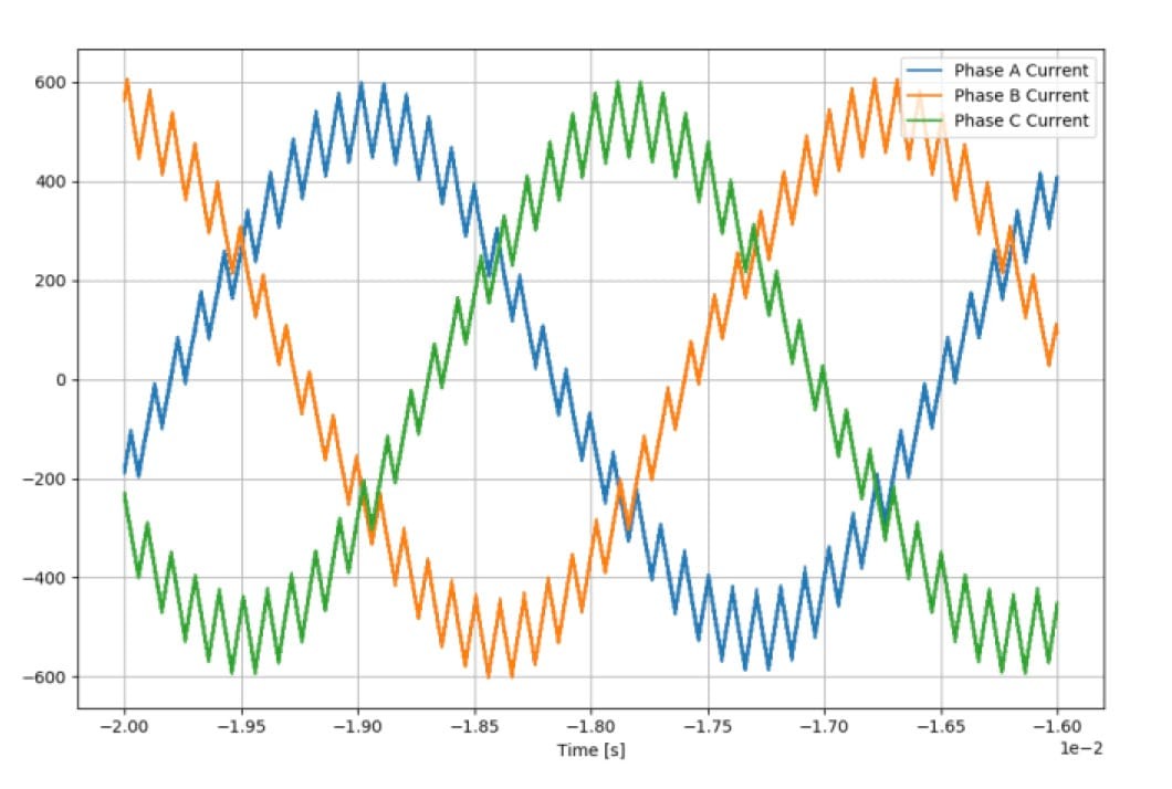
Full-power testing with three-phase load was conducted on the inverter with the same capacitor bank as the single-phase test bench and a three-phase inductor between the midpoint and each output of the inverter. A DC power supply was again used to supply the losses and was set to 800 V for the tests. The inverter was run at a fundamental frequency of 300 Hz and a switching frequency of 10 kHz with a load current of up to 360 ARMS, as shown in Fig. 15. With half the DC bus applied to the inductor, the 3-phase inverter processed a total of 300 kW of power. The total inverter losses for this test was approximately 2.8 kW
4 Conclusion
The XM3 Reference Design three-phase inverter maximizes the advantages of Wolfspeed’s C3M Silicon Carbide MOSFET technology in the high-performance XM3 power module package. The low-inductance of the XM3 package was continued through-out the inverter in the design of the bus bars and selection of capacitors. A high-performance thermal stack was designed capable of supporting the inverter up to 300 kW output with a power density of 32.25 kW/L. The inverter is fully instrumented with sensors, drivers, and controller to implement motor-drive or inverter applications. The fast, clean switching waveforms and low switching losses of the C3M MOSFET were demonstrated in addition to full power testing of the complete inverter.
5 References:
- A.Wijenayake, K.Olejniczak, D.Simco, S.Minden, M.Feurtado, et al.: Design of a 250 kW, 1200 V SiC MOSFET-Based Three-Phase Inverter by Considering a Subsystem Level Design Optimization Approach, ECCE, 2017.
- Wolfspeed Datasheet: CAS300M12BM2, 1.2kV, 4.2mΩ All-Silicon Carbide Half-Bridge Module, 2014.
- Infineon Datasheet: FF450R12ME4P_B11, 1.2kV, 450A, EconoDual3 Module, 2017.
- D. Martin, W. A. Curbow, B. Sparkman, L. E. Kegley, T. McNutt: Switching Performance Comparison of 1200 V and 1700 V SiC Optimized Half Bridge Power Modules with SiC Antiparallel schottky diodes versus MOSFET Intrinsic Body Diodes, APEC, 2017
- B.Kakarla, T.Ziemann, R.Stark, P.Natzke, U.Grossner: Short Circuit Ruggedness of New Generation 1.2 kV SiC MOSFETs, WiPDA, 2018