Maximize Efficiency in Isolated DC/DC Converters for EV Fast Charging Systems
Article
The global transition from internal combustion engine (ICE) vehicles to electric vehicles (EVs) requires significant advancements in the charging infrastructure required to support these vehicles. While low power (<15 kW) on-board chargers can support at-home charging during idle periods, extended trips and service industries require significantly faster charge times to match the speed of current gasoline refilling stops. Supporting these faster charge times requires a combination of both battery technology and charging infrastructure improvements. This guide discusses the design, development, and testing of a 60 kW dual active bridge (DAB) converter which can serve as both the isolation and regulation stages of an EV fast-charger. Furthermore, the topology selection enables this design to be paralleled to achieve output powers as high as 300 kW.
1. Introduction
Demand for electric vehicles (EVs) continues to grow worldwide as markets transition away from internal combustion engine (ICE) vehicles. The maturation of battery and power electronics technology has enabled EVs to be comparable to or better than ICE vehicles in a variety of performance metrics. However, a limiting factor in further market adoption continues to be suitable charging infrastructure to match the refilling capabilities of current ICE-based refueling solutions. Low-power (<15 kW) on-board chargers (OBCs) in EVs support long-duration charging during vehicle idle periods, such as in a garage overnight. However, these same chargers are not suitable for long road trips and commercial vehicle fleets where charge times need to be comparable to current ICE-fuel refilling times.
Standalone EV fast chargers (>50 kW) are necessary to achieve these required charge times and to further increase overall EV adoption. These chargers connect directly between the AC grid and the vehicle battery, bypassing the vehicle OBC, and thus creating a direct link which is capable of significantly higher power levels. This elevated-power output is often accomplished with relatively high voltages to avoid large high-ampacity cables. Though fast chargers can be larger than their onboard counterparts, fast chargers still need to achieve high efficiencies and high-power densities in order to scale to mass adoption.
Integrating silicon carbide (SiC) power electronics into EV fast chargers can enable the design to achieve all these demands (i.e., high output voltage, high efficiency, and high-power density). This white paper presents a 60 kW dual active bridge (DAB) converter building block to be used for EV fast charging. The topology selection and design decisions are discussed in detail, and the design is validated in both simulation and prototype hardware. Notably, this converter was designed to be paired with an active front end (AFE) to form a complete EV fast charger which can then be paralleled to achieve output powers as high as 300 kW.
2. Topology Selection
Since EV fast chargers are attached directly between the AC grid and the vehicle battery, for safe and reliable operation, these chargers must provide isolation to the user from the AC grid along with regulating the charger output voltage/current. The isolation could be achieved with a line-frequency transformer attached directly to the AC mains. However, at the power levels required for EV fast charging, this would result in a prohibitively large transformer. The capability of SiC power electronics to operate at high switching frequencies enables a high-frequency transformer to be adopted instead. High-frequency transformers offer the advantage of being significantly smaller than similarly rated low-frequency transformers. For this reason, a design was selected which utilizes a high-frequency transformer.
For a successful design, the AC grid must be rectified to a DC bus voltage to connect to a battery. This can be achieved with passive rectification using diodes, or through active rectification using topologies such as the AFE converter. The AFE provides significant benefits over passive rectification such as providing a regulated variable output voltage and enabling bi-directional power transfer. Though outside the scope of this white paper, the design discussed in this white paper assumes the input will be connected to an AFE-regulated DC bus voltage.
Several topologies can be paired with a high-frequency transformer to provide the required EV charger isolation. Some examples include the series resonant converter (SRC), LLC and CLLC (named for the components in their resonant tanks), phase shifted full-bridge (PSFB), and dual active bridge (DAB) [1]. The DAB topology was selected for this design for multiple reasons. First, the DAB can achieve zero-voltage switching (ZVS) in both the primary and secondary sides of the transformer across a wide-range of operating conditions. This reduces the overall system losses, leading to improved efficiency and reduced thermal management requirements. Second, the design supports bidirectional operation, which is critical for vehicle-to-grid applications where EV chargers can back-feed the AC grid. Third, the DAB can accomplish both the isolation and regulation requirements of a fast charger. When paired with an AFE, the entire charger is accomplished in just two-stages as shown in Figure 1. This prevents the requirement of including a third stage for providing the final output regulation (three-stage charger). Fourth, the DAB topology facilitates easy paralleling to provide a higher cumulative output power. In contrast, parallel operation with full-resonant topologies can be difficult since they often require precise matching of the switching frequencies between parallel stages. Parallel operation enables this DAB design to be used in a modular fashion by adding or subtracting parallel units to achieve varying maximum output power ratings.

Figure 1: Two-stage EV charger architecture
3. Dual Active Bridge (DAB) Converter Operation
The DAB converter uses a full-bridge circuit on both the primary and secondary sides of the transformer, as shown in Figure 2. Note that the figure includes more components which will be discussed later. Both full bridges operate in the same way, so only the primary-side devices will be discussed in detail, but the behavior is the same for the secondary-side devices. All the switch positions are operated using pulse-width modulation (PWM) with a 50% duty cycle (excluding the influence of deadtime). The diagonal switch positions of the full-bridge operate in-phase with each other; i.e., 𝐺𝑃1=𝐺𝑃4 and 𝐺𝑃2=𝐺𝑃3 The two sets of diagonal pairs, however, are 180 out of phase; i.e.:
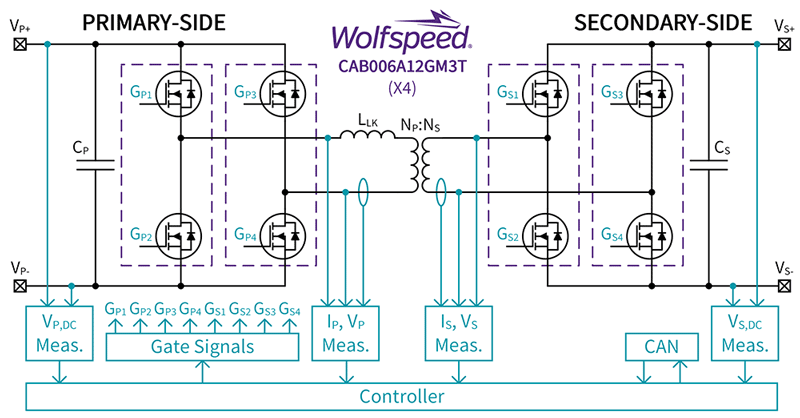
Figure 2: CRD60DD12N-GMA block diagram
This switching behavior occurs in both the primary and secondary sides of the transformer. The power transfer of the DAB occurs by introducing a phase shift between the primary and secondary transformer sides, as shown in Figure 3. By controlling the phase shift between the primary and secondary, the output power can be regulated, following
where POUT is the DAB output power [W], n is the transformer ratio [unitless], VP is the primary-side DC voltage [V], VS is the secondary-side DC voltage [V], ϕ is the phase shift [radians], fsw is the switching frequency [Hz], and Llk is the circuit leakage inductance [H]. Peak output power is achieved when ϕ= π/2. Notably, this control scheme only introduces a single phase shift between the primary and secondary. The DAB can be further improved by introducing independent phase shifts between the complementary diagonal pairs on the primary and between complementary diagonal pairs on the secondary (often referred to as triple-phase-shift (TPS) operation). However, these advancements are outside of the scope of this paper.
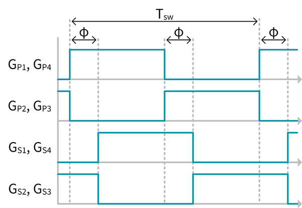
Figure 3: Single-phase shift timing diagram (deadtime omitted)
During the deadtime between complementary switching events, the stored energy in the DAB circuit leakage inductance discharges the semiconductor output capacitance. Assuming a properly designed circuit, this process discharges the semiconductor output capacitance to 0 V before the device is turned on. Since the device is turned at a 0 V, there is no voltage/current overlap during the turn-on process to create switching losses. This process, referred to as zero voltage switching (ZVS), is an advantage of the DAB topology and improves the circuit efficiency by reducing the system switching losses. When operating at rated load, the circuit can operate with ZVS in both the primary and the secondary sides.
4. Hardware
The hardware for this design is centered around the CAB006A12GM3T half-bridge power module, shown in Figure 4. This module features press-fit technology to easily integrate the module into a design through a simple press-in operation rather than bolting terminals or soldering large copper pours. Furthermore, this module uses a baseplate-less design which improves thermal performance by eliminating an element of the thermal stack-up of the module. The module is populated with all SiC MOSFETs in order to achieve the circuit level improvements offered by SiC power electronics discussed previously. Finally, this module uses pre-applied thermal interface material (TIM) which offers multiple benefits including: the TIM was specifically selected due to its enhanced performance compared to many off-the-shelf TIMs, the pre-application means that the TIM is always added consistently and reliably, and the thermal performance of the module with this TIM has already been extensively characterized by Wolfspeed®.
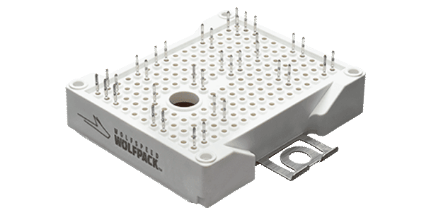
Figure 4: CAB006A12GM3T power module
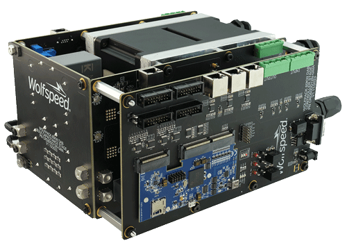
The realized design hardware is shown in Figure 5. The design uses four CAB006A12GM3T half-bridge power modules to create the full-bridge circuits on the primary and secondary sides of the transformer. The modules are mounted directly to liquid-cooled cold plate, and the plates are attached to two sides of the transformer to also provide cooling to the transformer. A high-frequency transformer with a 1:1 turns ratio, 248 μH of magnetizing inductance, and 5 μH of leakage inductance is used for the isolation. The design relies on just the leakage inductance of the transformer for ZVS and does not require a dedicated leakage inductor to be added to the circuit.
High-performance Wolfspeed CGD1700HB2M-UNA gate drivers are used to drive each half-bridge module, enabling high-speed operation, even at elevated bus voltages. Each position of the gate driver is isolated with an onboard isolated DC-DC power supply and the Texas Instruments® UCC21710 isolated gate driver integrated circuit. A Texas Instruments TMDSCNCD28379D general-purpose controller is employed for control to allow for easy firmware customization, and the design includes an integrated Controller Area Network (CAN) interface to provide a robust and reliable real-time communication with the controller for feedback and control updates. The design also includes voltage feedback measurements for monitoring input/output voltages and transformer current measurements for monitoring transformer bias currents.
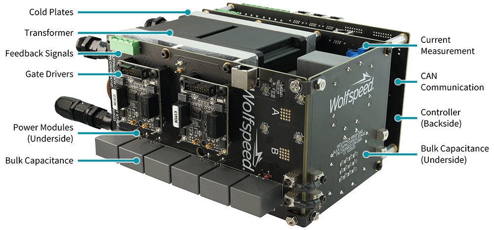
Figure 5: CRD60DD12N-GMA hardware
5. Experimental Validation
The system was experimentally validated at several operating conditions to demonstrate system operation. The performance at various load conditions was evaluated at the target switching frequency of 100 kHz. The full parameters of the experimental investigation are shown in Table 1. The system was operated open loop using a single phase shift. The experimental measurements were used to validate a variety of performance characteristics of the realized DAB circuit. First, the control of the phase shift was validated at power. The phase shift was manually controlled using a Wolfspeed graphical user interface (GUI), shown in the Figure 6(a). Figure 6(b) and Figure 6(c) show the measured gate-to-source voltages (VGS) and drain-to-source voltages (VDS), respectively, of one switch position on both the primary and secondary circuit sides. As expected, a configurable phase shift is measured between the primary and secondary switch positions in both the VGS and VDS measurements.
Parameter | VIN | VOUT | fSW | tdead | φ | POUT |
|---|---|---|---|---|---|---|
Value | 800 V | 800 V | 100 kHz | 200 ns | 3-20° | 10-60 kW |
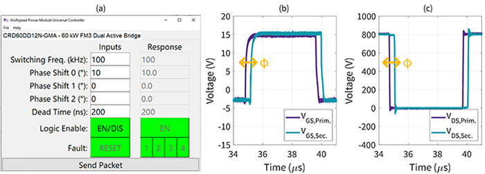
Figure 6: (a) DAB graphical user interface, and validation of phase shift in (b) VGS and (c) VDS measurements.
Second, the output regulation and transformer operation were evaluated at a high power using a resistor bank as the system load. Example time-domain measurements of the system operating at φ = 11.6° and POUT = 40 kW are shown in Figure 7. As shown in Figure 6, again the VGS and VDS phase shift are both apparent in the circuit measurements. Furthermore, the measurements indicate that the circuit is properly regulating the output voltage to a consistent 800 V (the target output voltage). Finally, the transformer current measurements follow the expected trapezoidal behavior characteristic of a dual active bridge circuit, indicating that the circuit is operating correctly.
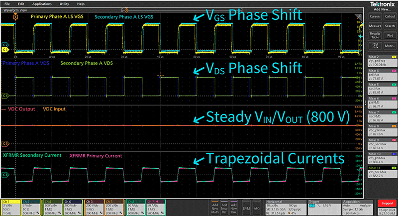
Figure 7: Example time-domain measurements at φ = 11.6° and POUT = 40 kW
Third, the system was checked for successfully achieving ZVS. Figure 8 shows VGS and VDS of one switch position on the primary and secondary sides while the circuit operated at φ = 18.9° and POUT = 60 kW (rated power). On both sides, the drain-to-source voltage reaches 0 V before the gate signals commands the device to turn-on, thus confirming the system is successfully operating under ZVS.
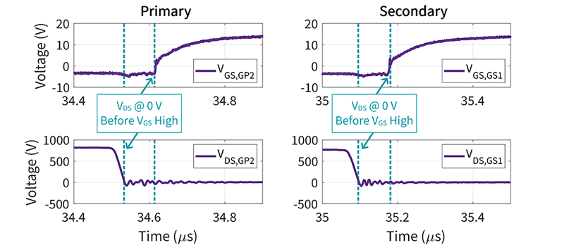
Figure 8: Validation of zero-voltage-switching turn-on
Fourth, the efficiency of the system was evaluated at various output power levels by changing the output load. The measured efficiency is shown in Figure 9. Since the system operates using SiC devices, the circuit is able to maintain a high level of efficiency across a wide range of output power levels (>98.7% efficiency when POUT ≥20 kW), and the circuit achieves a peak efficiency at 99.2%. Below 20 kW, the system no longer operates with ZVS resulting in an expected reduction of efficiency.
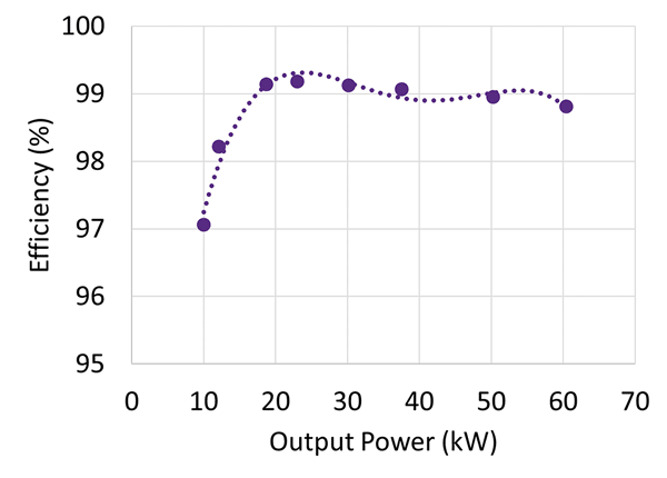
Figure 9: Measured efficiency
6. Simulation
Wolfspeed provides Plexim PLECS® models of all the power modules in the Wolfspeed portfolio, including the CAB006A12GM3T featured in this DAB design. These models are available here. Building upon these publicly available models, a full PLECS simulation, shown in Figure 10, was developed to capture the behavior of this DAB design. To check the validity of the model, the simulation was first exercised with the same operating conditions as the experimental results discussed previously, and the simulation shows strong agreement with the experimental results. For example, Figure 11 shows the primary and secondary transformer currents during 60 kW operation in both the simulation and experimental measurements. The simulation accurately captures the fundamental circuit behavior and measured magnitude observed in the experimental results.
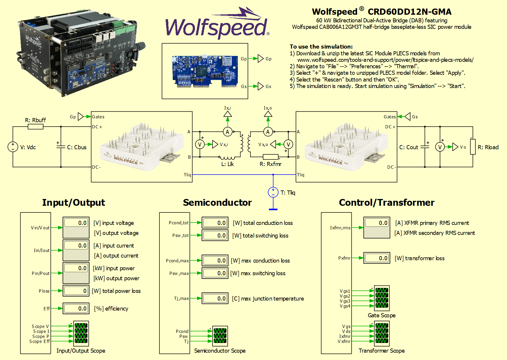
Figure 10: CRD60DD12N-GMA simulation
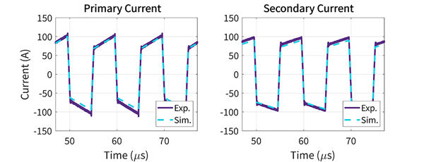
Figure 11: Simulation validation
Once demonstrated to model the general circuit operation, this simulation can be used to study the performance of various control strategies and to understand the sensitivity of included circuit parameters. For example, Figure 12 shows the impact of varying the leakage inductance on the primary transformer current. The simulation demonstrates that increasing the leakage inductance increases the peak primary transformer current in the system. Reducing the leakage inductance reduces the peak current. The simulation can be employed for further component optimization and controller strategies.
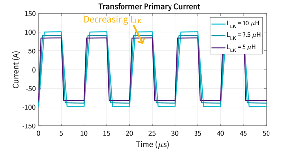
Figure 12: Simulation sensitivity analysis of transformer leakage inductance
7. Conclusion
This white paper presents a 60 kW dual active bridge converter which serves as a building block for an EV fast charger. The design is centered around the Wolfspeed CAB006A12GM3T half-bridge power module. The all-SiC power module features high-performance pre-applied thermal interface material, a baseplate-less design for improved thermal performance, and press-fit pins for easy module integration. When paired with an active front end, the modular DAB discussed in this document can be easily paralleled with more building blocks to scale the cumulative output power up to 300 kW. This white paper includes design operation fundamentals, hardware realization discussion, experimental validation, and simulation sensitivity analysis.
References
[1] B. W. Nelson, "Wolfspeed WolfPACK™ Power Module Platform: Accelerating Fast-Charger Development," Wolfspeed, 1 March 2021. [Online]. Available: https://www.wolfspeed.com/knowledge-center/article/wolfspeed-wolfpack-power-module-platform-accelerating-fast-charger-development/. [Accessed 7 May 2024].