Power modules: One shortcut to EMI compliance
Article
Electronic devices that are in proximity or share common conductors are susceptible to electromagnetic interference (EMI) that can disrupt their operation. Minimizing emissions is necessary to ensure that electrical systems do not interfere with each other’s normal operation when placed in the same environment. Power semiconductor devices, such as silicon (Si) IGBTs and silicon carbide (SiC) MOSFETs, are a common contributor of conducted EMI due to the fast switching required for their operation. During the switching transitions, the voltage across and current through the device rapidly changes states. The change between off and on states produces a dv/dt and di/dt that generates EMI at harmonic frequencies of the switching frequency.
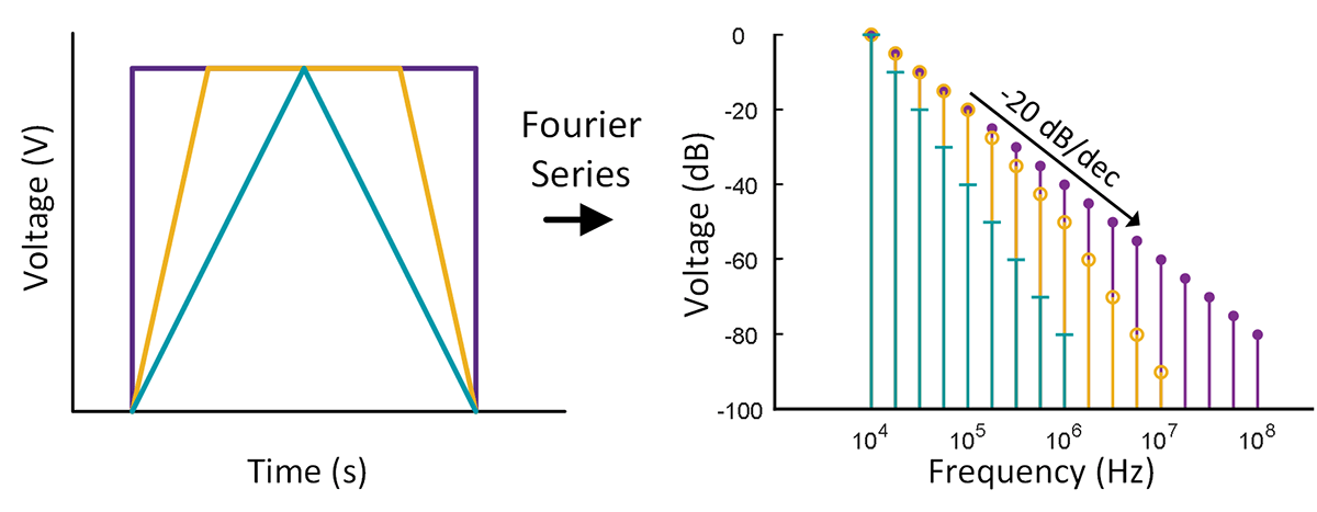
The switching frequency and edge rates (i.e., how fast the device changes state) determine the EMI generated during switching. Typically, the highest level of emissions will occur at the switching frequency and smaller peaks at integer multiples of the switching frequency. For example, if the switching frequency is 100 kHz, then the emissions spectra will have spikes at 100 kHz, 200 kHz, 300 kHz, and so on. The decay in spectral emissions across frequency for pulsed waveforms of varying rise times is illustrated in Figure 1. For an ideal square wave with infinite dv/dt and di/dt, the magnitude of the emitted spectra will decrease by 20 dB/decade. For an ideal triangle wave, which has the slowest possible dv/dt and di/dt, the spectra will decrease by 40 dB/decade. Thus, for the trapezoidal waveforms created by a power electronics device, the decay in spectra will decrease between 20 dB/decade to 40 dB/decade, the magnitude of which is determined by the edge rates. As devices are switched faster, it is expected that the emissions spectra at the harmonic frequencies will increase and decay slower across frequency.

This creates a series of tradeoffs for power electronics designers between switching frequency, edge rates, and EMI produced. In order to increase density, designers may opt to increase the switching frequency. This will reduce low-order harmonics but may increase emissions by shifting the spectral envelope toward higher frequencies. In addition, the more frequent switching will increase switching losses. To compensate for the overall increase in losses, designers may then opt to increase the edge rates (di/dt and dv/dt) in order to reduce switching losses. Unfortunately, the faster edge rates will in turn further increase the emissions of the system at higher frequencies. Thus, designers must consider the impact of EMI as applications increase switching frequencies and adopt high-performance, wide bandgap devices such as SiC.
Mitigation Methods
The overall emissions of a system are dependent not only on the switching of the power electronics, but also on how the generated noise couples to other systems. The goal is to contain the spectral content generated by the switching devices within the system or divert the emissions away from critical components. A common method of achieving this is to add EMI filters to the input and outputs of the power electronics; the filters allow desired content to pass freely, while redirecting or absorbing the unwanted content. However, EMI filters are bulky and expensive, and reducing their size is critical for optimizing cost and power density. A more efficient method is to consider coupling early during design. By strategically optimizing the small parasitic couplings within the system or by balancing passive components within the system around the parasitic couplings, emissions can be reduced significantly without using EMI filters. This provides designers another avenue to optimize their system and minimize emissions while still taking advantage of the efficiency and power density improvements offered by silicon carbide. However, this approach requires a deep understanding of the components and system that is not always intuitive to designers.
Impact of Heatsink Coupling
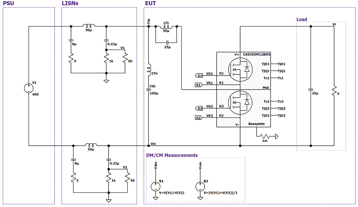
An important and prevalent parasitic coupling present in power electronic systems is the parasitic capacitance between the semiconductors and the heatsink. Generally, an electrically insulating but thermally conductive material is placed between the semiconductors and the heatsink. However, this effectively creates a small parallel-plate capacitance across the insulator where high-frequency common-mode currents can flow, providing an additional path for emissions to flow in the system. Figure 2 illustrates this concept. The equipment under test (EUT) describes the full converter or inverter system, and the line impedance stabilization networks (LISNs) are components used in compliance testing to provide a known input impedance to the system. During operation, high-frequency common-mode noise generated by the EUT can flow through the insulator capacitance of the semiconductors, to the baseplate, then to the heatsink, and then to other system components such as the LISNs.

This may result in elevated emission spectra that can cause an EUT to fail emission compliance testing. This situation matches many real-world systems, where the heatsink is commonly grounded for safety concerns and ease of implementation. Thus, applications must be designed considering this CM noise path to meet compliance requirements.
Advantages of Power Modules
Power modules provide advantages over discrete devices in their electrical and thermal characteristics, offering greater power density and in some cases simplifying assembly. One advantage is the use of a ceramic insulator to separate the high voltage conductors of the semiconductor devices and the metallic baseplate of the module. This allows modules to be attached directly to grounded heatsinks or other thermal management systems without additional insulation. In addition, because the ceramic properties and thickness are tightly controlled, power modules provide a consistent capacitance across samples. As such, the capacitive coupling of a module design can be quantified and is independent of the system it is implemented in. This is contrary to discrete devices, which often use insulating silicone pads that:
- May produce a capacitive coupling that varies across samples or mounting torque.
- Are dependent on the geometry of the system, rather than the semiconductor components, making it impossible to quantify until the full system is realized.
The consistent coupling value for power modules enables simulation and EMI mitigation opportunities in the design phase of a power converter. For power modules, the insulator capacitance between the semiconductors and the baseplate is known as the baseplate capacitance (BPC).
Distribution of Capacitance
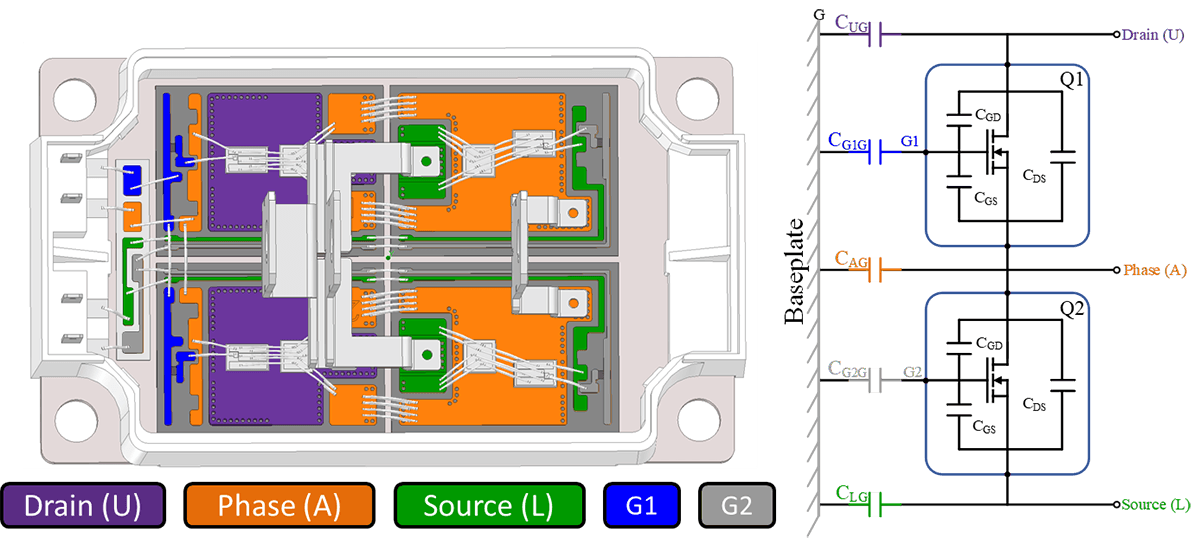
It is also important to understand the importance of the distribution of parasitic baseplate capacitances on EMI. In addition to the total baseplate capacitance, the ratio between these capacitances determines the overall common-mode emissions. In some cases, these capacitances can even be manipulated to specific ratios to significantly reduce common-mode current without the use of filters. An example of how baseplate capacitance is distributed in a Wolfspeed CAS175M12BM3 module is provided in Figure 3. Substrate regions are colored together if they are galvanically connected and should be modeled as a single lumped capacitance. Since the kelvin-source traces attach to the respective source pin at the top of the die, they are lumped together with the source node. Generally, the larger the area of the substrate region, the higher the capacitance coupling. For a half-bridge module, a full BPC model includes five baseplate capacitances: one for each power terminal, and one for each gate. This logic of separating individual baseplate capacitances can also be applied to any module topology.

EMI Simulation
Circuit-level simulation software (e.g., LTspice) is useful for studying the influence of parasitics and other parameters on EMI. Wolfspeed’s power module SPICE models are optimized for speed and accuracy, and include parasitic baseplate capacitance in the package model, allowing them to be used effectively for EMI simulations. It should be noted that, due to the complexity of small parasitic coupling between a system and the surrounding environment, it is difficult to perfectly predict emissions of a physical system. However, simulation can allow designers to study the influence of parasitic elements on emissions, or to experiment with filter designs. To demonstrate the influence of baseplate capacitance on EMI, the EMC boost converter simulation in Figure 4 was evaluated with and without the baseplate capacitances present in the package model.

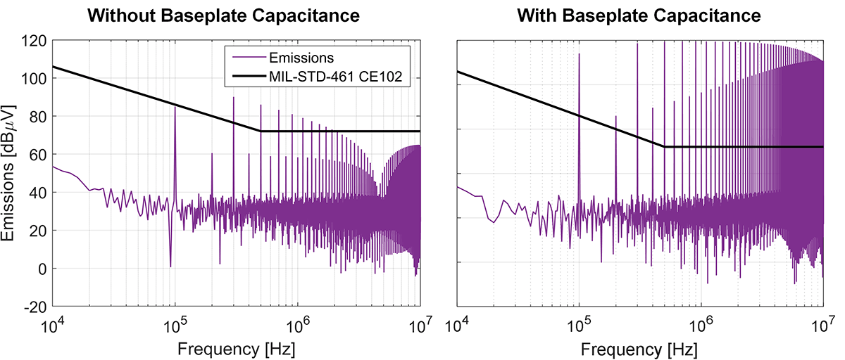
The spectral waveforms of V1 with and without baseplate capacitance are shown in Figure 5. The emissions limit for MIL-STD-461 CE102 is overlaid; any spectral content above this line indicates a compliance failure for this standard. While the system does not meet the EMC requirements in either configuration (which is not surprising, given the lack of EMI filter), the system with the baseplate capacitance has spectral content from 100 kHz to 10 MHz that lies above the emissions line. On the other hand, the system without baseplate capacitance is compliant above 2 MHz. It should be noted that this is an idealistic example; a physical system will have other common-mode paths in parallel with the baseplate capacitances.

From this position, designers can leverage the simulation to apply filters, evaluate the influence of parasitic couplings, investigate common-mode mitigation techniques, and further their understanding of their system before investing time and money into empirical compliance testing. However, this is only effective because the baseplate capacitances of power modules are known and included in the simulation. These quantities are measured and are published by Wolfspeed for all its power module platforms.