Silicon Carbide Modules Unlock Higher Power Density in Motor Drives
Article
The traction drive is where nearly all of an electric vehicle’s (EV’s) energy is put to use. The drive system must, therefore, perform with the highest possible efficiency while occupying the smallest possible space with the lowest weight — all to maximize the EV range. With the use of dual drives to enhance traction as well as an 800-V architecture to reduce losses, the industry needs inverters that increase output power from smaller size to deliver power density well beyond the capability of silicon (Si)-based technologies like IGBTs.
The latest generation of Wolfspeed’s Silicon Carbide (SiC) power modules are designed to meet these demands with lower losses, higher power density, and smaller size.
This paper presents the CRD600DA12E-XM3 three-phase dual inverter reference design and reveals how its components, including the CAB450M12XM3 power module and CGD12HBXMP gate driver, along with other key technologies, come together in a solution designed to enable next-generation EV traction.
A system overview
The CRD600DA12E-XM3 comprises two banks of CAB450M12XM3 power modules, each with CGD12HBXMP gate drivers (Figure 1). The overall design objective is to maximize performance through a high-ampacity, low-inductance design that is also low in cost and complexity.
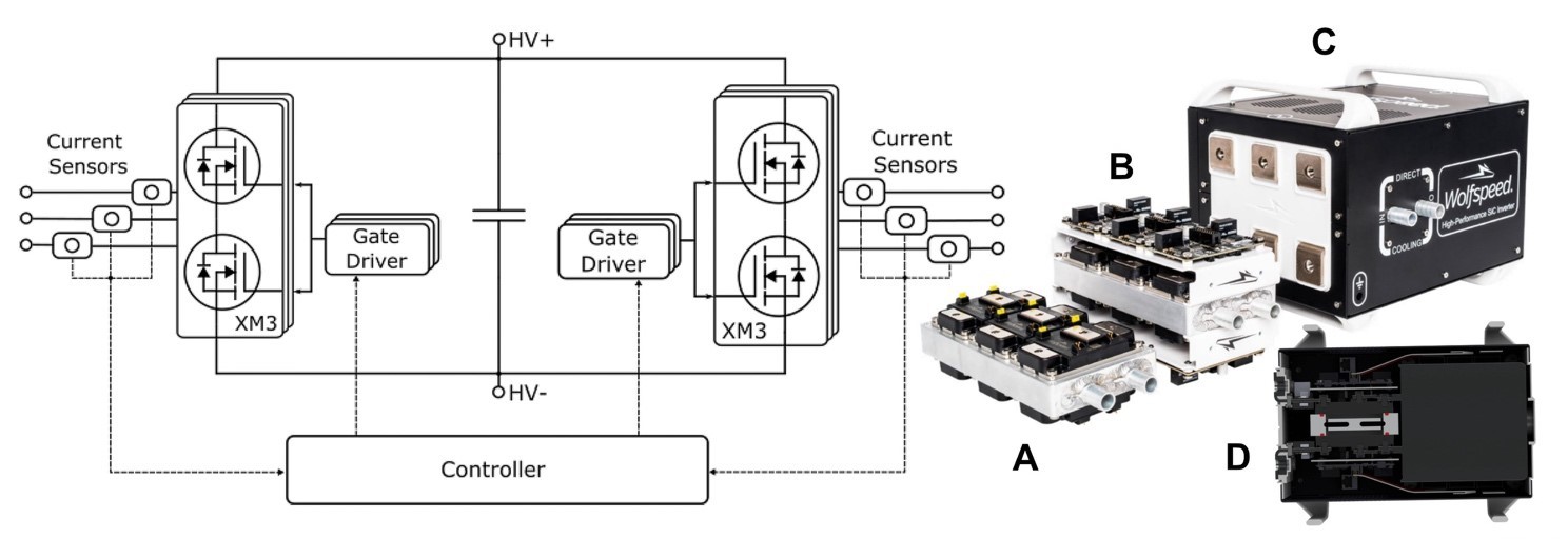
In designing the system, five key points needed to be considered:
- The high power density achievable from the use of Silicon Carbide (SiC) technology. Although Silicon Carbide (SiC) enables higher temperature operation, the high power density enabled requires that advanced heat-dissipation technologies be used.
- The fast switching speeds make the system more prone to overshoot and ringing caused by stray inductance; thus, stray inductance needs to be lowered from the busbar structure.
- This concern also demands low-inductance, high-ripple rating capacitance while keeping an eye on size reduction.
- The gate driver circuit must have adequate drive strength to sustain the switching speeds demanded and enabled by Silicon Carbide (SiC) technology.
- The overall power density should be significantly high to meet end-application requirements.
Power module platform of choice: XM3
A power module based on Wolfspeed’s XM3 full-Silicon Carbide (SiC) platform was the obvious choice because of its exceptional power density. Its weight and volume are about half as much as the standard 62-mm module, and the difference is even more dramatic against an EconoDUAL (Figure 2).
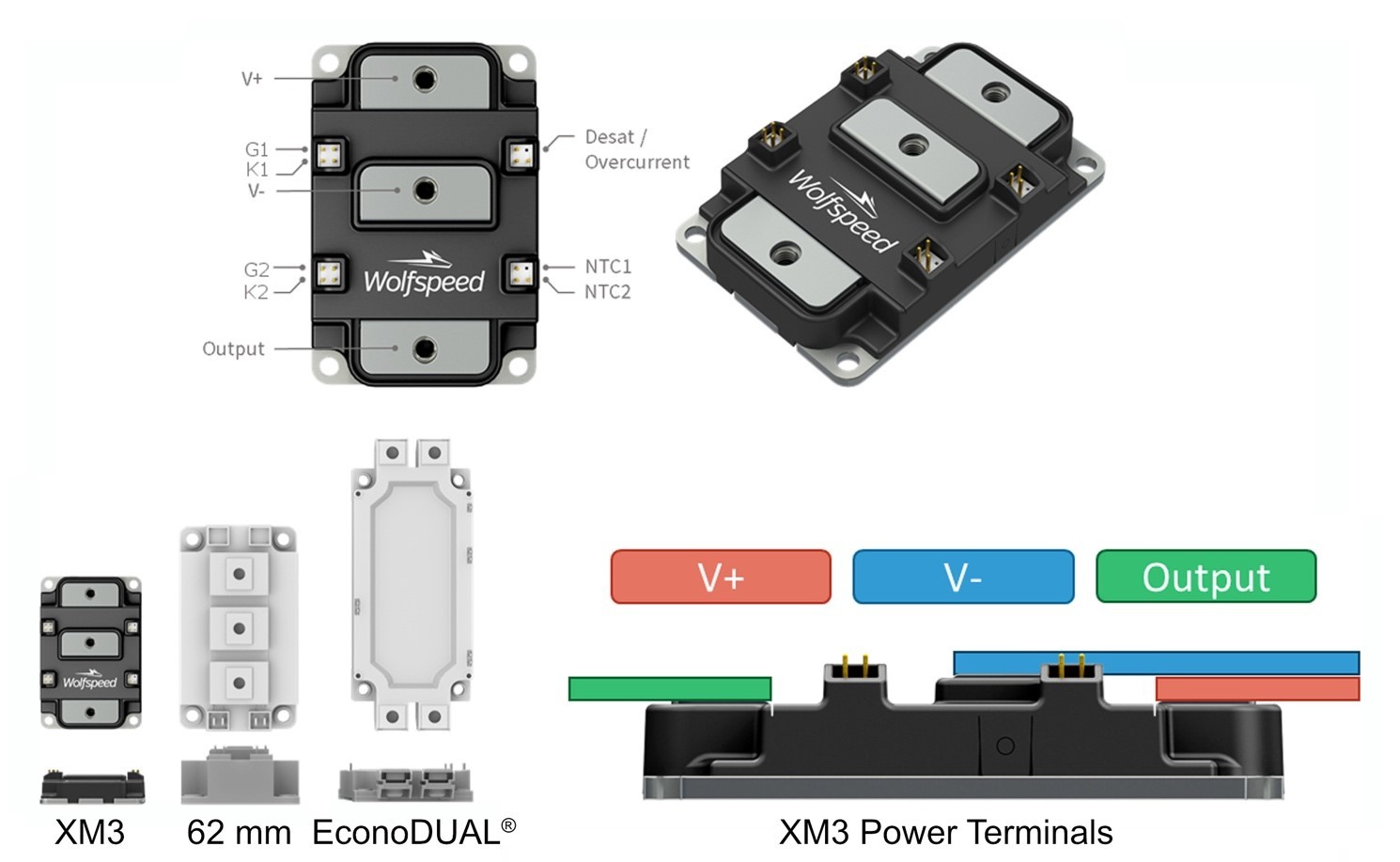
The XM3 platform is designed using an overlapping planar structure to achieve low stray inductance. The current loops within the module are wide and low-profile and yield even distribution between the devices, resulting in equivalent impedances across a switch position. The power terminals on the module are also vertically offset. This enables design of simple bussing between the DC-link capacitors and the module to be laminated all the way up to the module. The end result is a power-loop stray inductance of just 6.7 nH at 10 MHz.
The module features half the stray inductance of industry-standard modules and less than half the volume in a 53 × 80-mm footprint. The XM3 platform offers switching-optimized and conduction-optimized products for different target applications, such as the CAB450M12XM3 1,200-V, 450-A, half-bridge module used in this system.
The XM3 features include an integrated temperature sensor on the low-side switch position; built-in voltage sensing (de-sat) connection for easy driver integration; and a high-reliability silicon nitride (Si3N4) power substrate for enhanced power-cycling capability.
The inverter system performance is further enabled by several technologies, described below, to increase heat-dissipation efficiency, reduce parasitic inductance, and decrease component count as well as size.
The cold plate
The high current density enabled by Silicon Carbide (SiC) devices requires a high-performance thermal stackup to maximize heat transfer. Among the many options available in heatsinks, pressed copper tubes are the popular economical choice for liquid-cooled cold plates. While thin (~12.7 mm) copper-tube cold plates that support module mounting on both sides are available, they do have disadvantages of high thermal resistance that is different for the two sides, as well as high pressure drop, resulting in inconsistent cooling across the surface and on both sides.
The CRD600DA12E-XM3 instead uses Wieland Microcool’s micro-deformation technology (MDT) in the cold plate (Figure 3). MDT is a patented, low-cost, non-subtractive manufacturing process that mechanically and plastically deforms the work piece to form finite and repeatable micro-channels.

This is the basis of the high-performance cold plate with embedded channels that cool the full contact area of the XM3 module. The profile of the double-sided CP4012D-XP plate is optimized to match the XM3 module footprint with size reduction over the previous-generation CP3012.
A balanced coolant flow at a rate of 4 LPM across each of the six module positions results in an extremely low thermal resistance of 0.048°C/W per position or 0.008°C/W per cold plate. The cooling system has been tested up to 750-W power dissipation per switch with the CAB450M12XM3.
Driver strength
Because the Silicon Carbide (SiC) MOSFETs in the converter module are capable of high-power performance, the driver must have adequate drive strength — peak output current rating, or how much current is utilized to switch the devices on and off — to sustain fast switching speeds. A >10-A rating is recommended to ensure high edge rates. And Wolfspeed’s CGD12HBXMP gate driver delivers.
The two-channel gate driver is protected against overcurrent and reverse polarity and has on-board 2-W isolated power supplies to support 80-kHz switching frequency. Its user-configurable turn-on and turn-off gate resistors enable switching loss optimization.
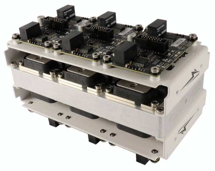
The driver also features tunable overcurrent detection with soft-shutdown, undervoltage lockout as well as anti-overlap of PWM inputs. It also offers ~2-µs inception to extinguish time to safely shut down under a short-circuit.
Because Silicon Carbide (SiC) MOSFETs have a high dV/dt rate, an inadequate common-mode transient immunity (CMTI) rating can permit latch-through between the logic and driver output, causing hardware failure. The CGD12HBXMP offers a high, 100-kV/μs CMTI rating, low (<5 pF) isolation capacitance, and differential inputs for increased noise immunity.
The CGD12HBXMP also shares the same footprint as the XM3 module, allowing for a compact power core to be formed with six CAB450M12XM3 modules and their drivers integrated on the cold plate (Figure 4). This then becomes a compact solution for easy integration into dual-inverter designs.
DC-link capacitor
Reduction in parasitic inductance is a key concern, and as mentioned earlier, it is partly reduced by the vertically offset power terminals on the XM3 modules to simplify busbar design and lower power-loop inductance. This concern is further addressed in the choice of the DC-link capacitor that is shown in Figure 5.
The capacitor footprint is one of the biggest obstacles to increasing power density. Off-the-shelf six 100-µF cylindrical capacitors would normally be used to achieve the required ripple current rating, occupying a 451-cm2 footprint and requiring a separate busbar.
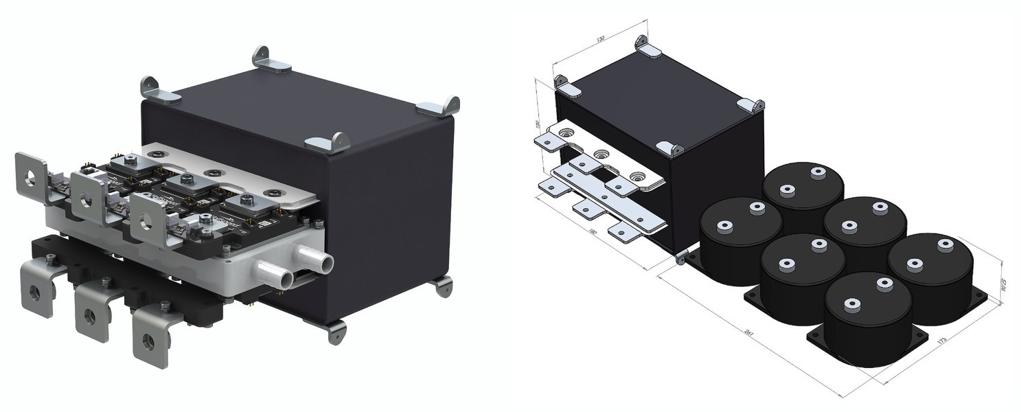
Wolfspeed instead used a custom-designed DC-link capacitor (Figure 5) with a compact footprint of just 234 cm2. It features integrated laminated bussing connected to the power terminals of the XM3 power modules on both sides of the cold plate, which reduces the parasitic inductance in the power loop and ensures a balanced current path for both sets of modules. Component count is reduced as well by eliminating separate bus bar and hardware.
The custom capacitor is 600 µF at 900 V with a peak voltage rating of 1,200 V. Because the capacitor-and-integrated-busbar stray inductance are critical to reduce voltage spikes under the high di/dt rates common in fast-switching Silicon Carbide (SiC) inverters, the design was validated with an impedance analyzer that measured 13-nH equivalent series inductance at the terminals. Combined with the 6.7-nH inductance from the XM3 module, a total power-loop inductance of just 20 nH is achieved, allowing for faster switching speeds to be used.
The controller
The selection of the processor for the controller board in this system needed to be based on the following considerations:
- It should have enough processing “horsepower” to sample all inputs and make control decisions.
- It should have a high-enough ADC count to enable all the required system states to be measured for appropriate control and monitoring.
- It should have fast hardware interrupts to respond to fault conditions.
- It must support standards-based communications critical for proper operation.
The system’s controller board therefore uses a dual-core, floating-point, 200-MHz, 32-bit DSP from Texas Instruments. The DSP has enough ADC inputs to measure current, voltage, and temperature and offers communication support, including isolated CAN.
Current sensors
The dual inverter uses six current sensors at the output terminals. With that number of sensors in the system, any size reduction in the sensor modules chosen quickly becomes significant. Although COTS current sensor modules are easily available, they can be bulky. Moreover, some of the three-in-one sensor modules on the market add constraints to the bussing geometry.
For the CRD600DA12E-XM3 system, Wolfspeed chose the DC-to-250-kHz Melexis MLX91208 Hall-effect sensor to provide a high-speed analog output signal proportional to the external horizontally applied flux density, with a response time as low as 3 µs.
The sensor is packaged in an eight-pin SOIC and is small enough to be mounted onto a compact PCB that can then be attached directly to an output busbar. The flexibility of the PCB mount allows simplification of the output bussing.
Moreover, the MLX91208 uses an integrated magneto-concentrator (IMC) deposited on the CMOS die, which eliminates the need for a large ferromagnetic core (Figure 6). This assembly occupies 91.6 mL against the 800-mL volume of another popular sensor assembly used in the automotive industry.
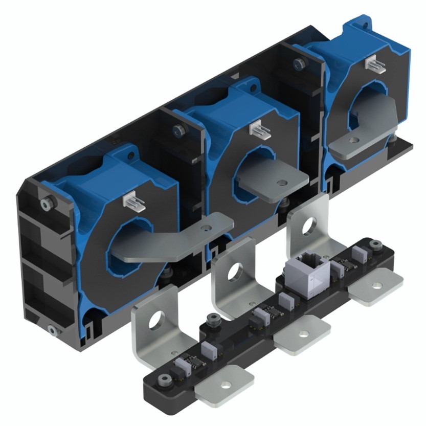
The high dV/dt rates typical in Silicon Carbide (SiC) inverters can create noise on sensitive low-voltage signals, such as those from current sensors. The current sensor’s proximity to the switching nodes makes them even more susceptible. This is true as well for the cabling between the sensor and the controller, which can pick up the noise as it is routed around the system.
The sensor chosen by Wolfspeed requires only a laminated U-shaped magnetic shield to protect against external fields and homogenize the field. A ground layer in the PCB blocks capacitive coupling from the busbar to the sensor. The use of differential signaling significantly reduces the impact of radiated noise from the switching. Additionally, using shielded, twisted-pair CAT6 cabling between the sensor boards and the controller ensures that any noise is common-mode on both signals of the differential pair.
Testing performance
A clamped, inductive-load, double-pulse test was conducted under aggressive switching conditions using a low gate resistance to validate the entire power loop. The constant current load waveforms showed a turn-on switching energy of 23.1 mJ at 800 V and 600 A, with a peak current overshoot of 113 A.
The turnoff switching energy was 30.1 mJ. The margin of the bus voltage for the die was 80 V, which is at a 2× overload condition compared with the nominal rating of the module.
Next, switching losses per module were calculated from the known turn-on energy of 12.2 mJ and turn-off energy of 12 mJ at the 300-A nominal condition. Using the formula for switching power loss (PSW),
and plugging in the EON and a switching frequency (fSW) of 10 kHz,
this loss is 3× lower than a comparable Si IGBT (HybridPack 1,200 V, 380 A nominal), with Silicon Carbide (SiC) having the big advantage of an extremely low reverse-recovery energy (ERR).
The design was also validated under application conditions using a three-phase recirculating load test.
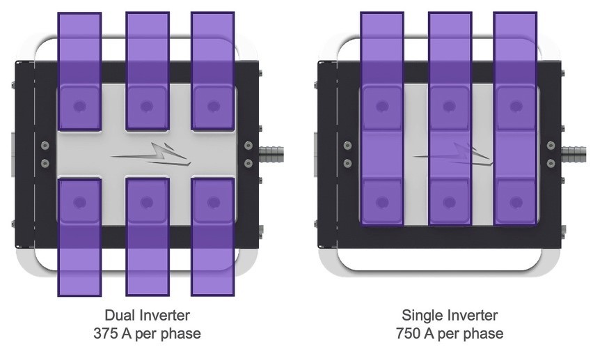
The design’s flexible arrangement of output terminal eased test setup — the six outputs can be utilized either as two independent three-phase inverters delivering 375 ARMS each or, with the addition of a simple bus bar and paralleling of phases, as a single three-phase inverter capable of 750 ARMS (Figure 7).
For the test, the single inverter setup was used with AC outputs U and X combined to form Phase A, V and Y Phase B, and W and Z Phase C. Three 125-µH load inductors were connected between one of the output terminals of the inverter and the midpoint of a large capacitor bank — 2.2 mF per half — rated to 1,100 V.
This enables high-power testing with only a few kilowatts of power supplied and with the DC voltage source only supplying the system losses. Energy is transferred from one-half of the capacitors to the other half through the inductors during each switching cycle, and the direction of energy transfer is reversed over one cycle of fundamental frequency.
After a five-minute test at 800-V bus voltage, the capacitor case reached 13°C above ambient, while the gate driver hot spot measured 40°C above ambient. For a switching frequency of 10 kHz and a fundamental frequency of 300 Hz, the RMS paralleled output current was 750 A, equivalent to 624 kW of output power. The current ripple with the chosen load inductor was 160 A at 10 kHz, while the peak combined current reached 1,200 A, including the current ripple.
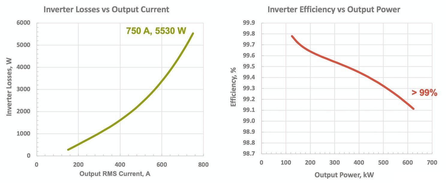
The switching energy at 10 kHz, 375 A was 31 mJ. For the total losses of 5.53 kW or 460 W per switch, the switching losses were 1.8 kW. This results in an efficiency exceeding 99% for the inverter up to 624 kW (Figure 8).
The final word
Meeting the five key design considerations set out earlier, the CRD600DA12E-XM3 three-phase dual inverter reference design utilizes the CAB450M12XM3 power modules to achieve a peak output power of 624 kW and a current rating of 375 Arms per phase or 750 Arms paralleled.
Competitor | CRD300DA12E-XM3 | CRD600DA12E-XM3 | |
|---|---|---|---|
Semiconductor | Si IGBT | SiC | SiC |
Type | Single Inverter | Single Inverter | Single Inverter |
Output Power | 250 kW | 300 kW | 624 kW |
Volume | 12.6 L | 9.3 L | 8.6 L |
Power Density | 19.8 kW/L | 32.2 kW/L | 72.5 kW/L |
Table 1: The CRD600DA12E-XM3 Achieves a Power Density Of 72.5 Kw/L, Which Is 3.6× Higher Than That Possible With an Equivalent-Rated IGBT Design.
In the full-metal 204 × 267.5 × 157.5-mm enclosure (shown in Figure 1), this solution weighs 9.7 kg and occupies merely 8.6 L in volume to reach the exceptionally high power density of 72.5 kW/L. This is more than double that achieved by the previous 300-kW Silicon Carbide (SiC) reference design and 3.6× better than what is possible with an equivalent-rated IGBT-based inverter (Table 1).
To find out more about the CRD600DA12E-XM3 three-phase dual inverter reference design, the CAB450M12XM3 power module, and the CGD12HBXMP gate driver, contact Wolfspeed’s Power Team.