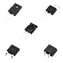
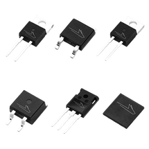
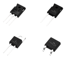
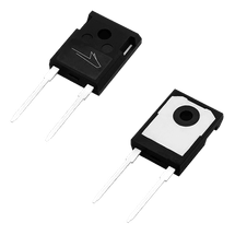
Discrete Silicon Carbide Schottky Diodes
Further reduce conduction losses with ultra-low voltage drop Schottky diodes in power rectifier applications, or any circuit that requires protection from reverse current.
Products
No filters selected, showing all 50 products
Filter By
Product SKU | Buy Online | Request Sample | Data Sheet | CAD Model | Status | Blocking Voltage | Current Rating | Forward Voltage(VF(type)) | Maximum Continuous Current (IF) | Package | Qualification | Generation |
|---|---|---|---|---|---|---|---|---|---|---|---|---|
Active | 600 V | 2 A | 1.5 V | 2 A | TO-252-2 | Industrial | Gen 3 | |||||
Active | 600 V | 4 A | 1.5 V | 4 A | TO-252-2 | Industrial | Gen 3 | |||||
Active | 600 V | 4 A | 1.5 V | 4 A | TO-220-F2 Full | Industrial | Gen 3 | |||||
Active | 600 V | 4 A | 1.5 V | 4 A | TO-220-2 | Industrial | Gen 3 | |||||
Active | 600 V | 6 A | 1.5 V | 6 A | TO-220-F2 Full | Industrial | Gen 3 | |||||
Active | 600 V | 6 A | 1.5 V | 6 A | TO-220-2 | Industrial | Gen 3 | |||||
Active | 600 V | 8 A | 1.5 V | 8 A | TO-263-2 | Industrial | Gen 3 | |||||
Active | 600 V | 8 A | 1.5 V | 8 A | TO-220-2 | Industrial | Gen 3 | |||||
Active | 600 V | 10 A | 1.5 V | 10 A | TO-263-2 | Industrial | Gen 3 | |||||
Active | 600 V | 10 A | 1.5 V | 10 A | TO-220-2 | Industrial | Gen 3 | |||||
Active | 600 V | 20 A | 1.5 per leg | 20 A | TO-247-3 | Industrial | Gen 3 | |||||
Active | 650 V | 4 A | 1.5 V | 4 A | TO-220-2 | Industrial | Gen 3 | |||||
Active | 650 V | 4 A | 1.27 V | 4 A | TO-252-2 | Industrial | Gen 6 | |||||
Active | 650 V | 4 A | 1.27 V | 4 A | TO-220-2 | Industrial | Gen 6 | |||||
Active | 650 V | 6 A | 1.27 V | 6 A | QFN 8x8 | Industrial | Gen 6 | |||||
Active | 650 V | 6 A | 1.5 V | 6 A | TO-252-2 | Industrial | Gen 3 | |||||
Active | 650 V | 6 A | 1.27 V | 6 A | TO-252-2 | Industrial | Gen 6 | |||||
Active | 650 V | 6 A | 1.27 V | 6 A | TO-220-2 | Industrial | Gen 6 | |||||
Active | 650 V | 8 A | 1.27 V | 8 A | QFN 8x8 | Industrial | Gen 6 | |||||
Active | 650 V | 8 A | 1.5 V | 8 A | TO-220-2 | Industrial | Gen 3 | |||||
Active | 650 V | 8 A | 1.27 V | 8 A | TO-252-2 | Industrial | Gen 6 | |||||
Active | 650 V | 8 A | 1.27 V | 8 A | TO-220-2 | Industrial | Gen 6 | |||||
Active | 650 V | 8 A | 1.5 V | 8 A | TO-220-2 Isolated | Industrial | Gen 3 | |||||
Active | 650 V | 10 A | 1.27 V | 10 A | QFN 8x8 | Industrial | Gen 6 | |||||
Active | 650 V | 10 A | 1.27 V | 10 A | TO-263-2 | Industrial | Gen 6 | |||||
Active | 650 V | 10 A | 1.5 V | 10 A | TO-220-2 | Industrial | Gen 3 | |||||
Active | 650 V | 10 A | 1.27 V | 10 A | TO-252-2 | Industrial | Gen 6 | |||||
Active | 650 V | 10 A | 1.27 V | 10 A | TO-220-2 | Industrial | Gen 6 | |||||
Active | 650 V | 10 A | 1.5 V | 10 A | TO-220-2 Isolated | Industrial | Gen 3 | |||||
Active | 650 V | 16 A | 1.27 V | 16 A | TO-247-3 | Industrial | Gen 6 | |||||
Active | 650 V | 16 A | 1.5 V | 16 A | TO-220-2 | Industrial | Gen 3 | |||||
Active | 650 V | 20 A | 1.27 V | 20 A | TO-263-2 | Industrial | Gen 6 | |||||
Active | 650 V | 20 A | 1.27 V | 20 A | TO-247-2 | Industrial | Gen 6 | |||||
Active | 650 V | 20 A | 1.27 V | 21 A | TO-220-2 | Industrial | Gen 6 | |||||
Active | 650 V | 20 A | 1.27 V | 20 A | TO-247-3 | Industrial | Gen 6 | |||||
Active | 650 V | 30 A | 1.35 V | 88 A | TO-247-2 | Industrial | Gen 6 | |||||
Active | 650 V | 30 A | 1.5 V | 30 A | TO-247-3 | Industrial | Gen 3 | |||||
Active | 650 V | 50 A | 1.3 V | 50 A | TO-247-2 | Industrial | Gen 6 | |||||
Active | 650 V | 50 A | 1.3 V | 50 A | TO-247-3 | Industrial | Gen 6 | |||||
Active | 1200 V | 2 A | 1.4 V | 2 A | TO-252-2 | Industrial | Gen 4 | |||||
Active | 1200 V | 5 A | 1.4 V | 5 A | TO-252-2 | Industrial | Gen 4 | |||||
Active | 1200 V | 5 A | 1.4 V | 5 A | TO-220-2 | Industrial | Gen 4 | |||||
Active | 1200 V | 10 A | 1.5 V | 10 A | TO-252-2 | Industrial | Gen 4 | |||||
Active | 1200 V | 10 A | 1.4 V | 10 A | TO-247-3 | Industrial | Gen 4 | |||||
Active | 1200 V | 10 A | 1.5 V | 10 A | TO-220-2 | Industrial | Gen 4 | |||||
Active | 1200 V | 20 A | 1.5 V | 20 A | TO-247-2 | Industrial | Gen 4 | |||||
Active | 1200 V | 20 A | 1.5 V per leg | 20 A | TO-247-3 | Industrial | Gen 4 | |||||
Active | 1200 V | 20 A | 1.5 V | 20 A | TO-220-2 | Industrial | Gen 4 | |||||
Active | 1200 V | 30 A | 1.5 V | 30 A | TO-247-2 | Industrial | Gen 4 | |||||
Active | 1200 V | 30 A | 1.6 V per leg | 30 A | TO-247-3 | Industrial | Gen 4 |
Knowledge Center
Silicon carbide is revolutionizing the heat pump and air conditioning industry by delivering unprecedented efficiency, enhanced durability, and superior performance in the most challenging of environments.
Use the SpeedFit™ Design Simulator to design smaller and quieter industrial motor drive systems including industrial low voltage motor drives, servo drives, and compressors for heat pumps and air conditioners.


