Thermal Solutions for Surface Mount Power Devices
Article
Abstract
The first part of the paper presents a Printed Circuits Board (PCB) thermal vias design recommendations for surface mount (SMT) power devices for relatively low power applications. Simulation is conducted to compare different thermal vias arrays. A PCB with different thermal vias array is fabricated, and thermal impedance is measured. The measured result confirms simulation results.
The second part of the paper introduces an innovative ceramic-embedded Alumina Nitride (AlN) FR4 PCB solution for surface mount power devices in high power applications. This embedded AlN PCB solution provides excellent thermal conduction, and electrical isolation at same time. A simulation work is also conducted. And PCB is manufactured to verify the simulation result. Finally, a 6.6kW EV on-board charger power converter is developed based on this AlN-embedded PCB.
Introduction
A surface mount package is a very common power package for power application, since it is easier for manufacturing automation. However, surface mount devices present a challenge in thermal management. Printed Circuits Boards(PCB) have low thermal conductivity due to properties of dielectric laminates. The most cost-effective way is to apply thermal via arrays on PCBs for low power applications. However, determining how to select the array pattern to maximize the thermal performance is not trivial task. Most of reference [1][2][3] discussed the thermal vias designs for vias underneath the thermal source directly. However, there is an issue by applying copper-plated thermal vias on PCB board [1], as shown in Fig. 1. As thermal vias are under the solder pad of devices, solder flows into vias during reflow process. This introduces defects in solder joints of devices. Consequently, lifetime of the solder joints is reduced. To avoid this problem, people can fill the vias with some filler material. However, this is not a standard process. The work in first part of this paper is to arrange the thermal vias around the power device. The goal is to arrange the vias so that it can transfer max heat.

Based on the information from literature and manufacturers[2][3], the hole size of thermal vias is fixed at 0.3mm diameter, with 1.0mm center-to- center distance in the array seemed to be a very good choice. We only needed to decide how many rows on each side of device. Different array patterns are selected and simulated. To verify the simulation, PBC with different thermal vias are fabricated and the thermal impedance is measured.
For higher power applications, it is difficult to use the thermal vias since they have too high a thermal impedance. A common approach is to use an insulated metal substrate (IMS) base PCB solution[4], but the PCB layout is limited by the single layer metal base PCB. In addition, the thermal conductivity of the PCB is limited, so the power density of the system is also limited. Recently, a new hybrid substrate technology emerged in the market[5]. With this technology, an AlN slug can be embedded in a specific area of PCB. A multi-layer PCB can still be used for a complicated system, such as the conventional multi-layer PCB. A simulation work for this AlN inlay PCB is performed, and a PCB is also fabricated to verify the result.
The paper is organized in following way; In section 2, the thermal vias simulation and PCB board verification are described. In section 3, the PCB with AlN inlay is described and simulated. The PCB is manufactured to verify the simulation. Finally, a 6.6kW bi-directional EV on board charger is designed based on AlN inlay PCB technology.
Thermal Vias Design
Since the thermal vias under the devices will cause solder flowing into vias, which will introduce undesired soldering problem, in this study, the thermal vias are arranged around the surface mount device as shown in Fig.3. The goal is to find out what is the best pattern for thermal conductivity in terms of thermal impedance: how many vias in X and Y dimensions. Based on the information from literature and manufacturers, the hole size of thermal vias is fixed at 0.3mm diameter, with 1.0mm center to center distance in the array.
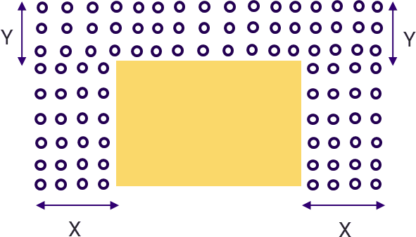
Different array patterns are selected and simulated. The simulation work is targeting for D2PAK. A 7 lead D2PAK SiC MOSFET is modeled in the simulation and PCB with 2 copper layers is used. Cu layer thickness is 2oz(~60mil), and overall thickness of PCB is 1.6mm. Different via patterns are arranged as 5, 10 rows on the other three sides of the device. The third pattern is that vias fill entire copper area 1 × 1 in2. The patterns for comparison are shown in Fig. 4, which only half of the array is shown since it is symmetrical.

All the materials involved in the simulation, as shown in Table 1.
Materials | Thermal Conductivitty W/m × L | Specific Heat J/kg × K | Density kg/m³ |
|---|---|---|---|
SiC | 4900 | 750 | 3.1e3 |
Solder | 50 | 167 | 8.4e3 |
Copper | 386 | 380 | 8.954e3 |
Molding Compound | 0.99 | 820 | 1980 |
FR4 | 0.3 | 950 | 1.8e3 |
Air | 0.0257 | 100.75 | 1.205 |
AIN | 170 | 740 | 3260 |
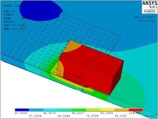
The following simulation picture shows the heat spread in model B. The simulation boundary condition is fixed bottom convection coefficient 1200W/m2K. The loss of the power device is 6W. The heat spread up to the 10th via, but it is significantly reduced after 6th via. The simulation heat spread image is shown in Fig.5. The heat doesn’t spread to all vias, which means more vias simply don’t help.
The simulation result is shown in the following table 2. ϴboard Is the thermal impedance of the PCB board through thermal vias.
Case | ϴjunction-case °C/W | ϴsolder °C/W | ϴboard °C/W |
|---|---|---|---|
A | 0.51 | 0.02 | 3.92 |
B | 0.51 | 0.02 | 3.62 |
C | 0.51 | 0.02 | 3.92 |
To verify the thermal model and simulation results, PCB with 3 patterns are fabricated, and thermal resistance of PCBs with designed via arrays are measured experimentally.
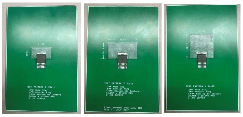
It was found that the measured results were all around 4°C/W. Due to variations and other uncontrolled factors during measurements, the measurement results do not perfectly fit the simulation results. But measurement result is within close range compared with simulation results.
From the simulation and experiment result, the thermal impedance from thermal vias is high, which is expected. It is only good for low power applications.
Based on this study, the recommendations for thermal vias array design include:
- Avoid via placed under drain tab to prevent solder wetting through via, which may weaken solder joint reliability.
- Via size is recommended with 0.3mm diameter with 1.0mm center-to-center distance in the array. Via size and spacing can vary depending on manufacturing capability.
- Thermal via with 35µm Cu is recommended with better thermal performance and limited additional cost in fabrication.
- In the via array, via evenly distributed in all three directions can contribute more to reducing thermal impedance, thus providing better thermal performance compared with larger 1.0 × 1.0 in2 thermal via array.
- Heat spreading in thermal via array is limited to 10mm from each edge of the device, with the same parameters in this work. Thermal via array with at least 5 via extended from each edge of the device is recommended, but more than 10 via is not helpful.
Embedded AlN PCB Design
For high power applications, like an EV battery on board charger or off board charger, it is impractical to use thermal vias for heat transferring. Another approach is to use an insulated metal substrate (IMS) base PCB solution[4], but the PCB layout is limited by the single layer metal base PCB. Control signals have to come from another PCB through connectors which could cause reliability issues. In addition, the thermal conductivity of the PCB is limited, so the power density of the system is limited. A new ceramic-embedded (AlN) FR4 PCB has been used in LED applications[5]. AlN provides good electrical isolation and thermal conductivity at the same time. Regular multi-layer PCB design can still be employed for complex circuitry, but there is no literature to use this AlN inlay PCB for power application.
Therefore, a PCB with AlN is simulated. The modeling of embedded AlN PCBs is similar with the modeling in thermal via PCB models. The only difference is that embedded thermal conductive AlN blocks are between top and bottom Cu pads on PCBs instead of thermal vias.
The AlN block is 6.5mm × 10.5mm and the thickness is 1.6mm. The simulation result in Fig.7 shows almost no heat spread. The heat is transferred directly to the bottom of PCB through the AlN block.
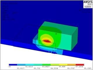
The simulation shows the AlN block provides thermal impedance 0.21 °C/W. A prototype PCB with AlN is built, as shown in Fig.8. The AlN block is under the square landing pad of the power device, size 6.5mm × 10.5mm.
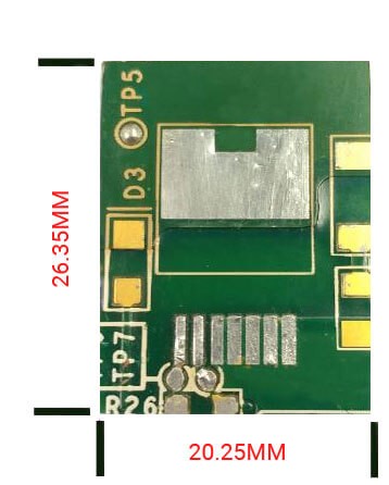
Lab testing results confirm the thermal impedance of AlN PCB 0.23 °C/W. This AlN-embedded PCB is excellent for high power application since it not only has very low thermal impedance, it also provides electrical isolation. Because it is integrated with regular multi-layer PCB, it can increase power density more than the IMS solution. A 6.6kW bi-directional EV on-board charger was designed based on this AlN- embedded PCB technology[6]. It successfully provides good thermal management with peak system efficiency >96.5% for such high power application. More detail can be found in the reference paper[6].

Conclusions
This paper presents a recommended thermal vias pattern for SM power devices in low power applications. The thermal vias design is compatible with standard manufacturing process. For high power applications, an innovative AlN- embedded PCB is simulated and experimented. Its excellent thermal performance is very promising for high power application in multi-kW power converter. A 6.6kW SiC MOSFET based bi- directional EV on boarder charger was built to demonstrate the performance of AlN-embedded PCB technology.
References
- Cree Application note, Optimizing PCB Thermal Performance for Cree XLamps LEDs.
- Deepak Gautum, “A Comparison of Thermal Vias Patterns used for Thermal Management in Power Converter,” 2013 IEEE Energy Conversion Congress and Exposition.
- N. Kafadarova, A. Andonova, PCB Thermal Design Improvement Through Thermal Vias. Recent Advances in Circuits, Systems, Electronics, Control and Signal Processing.
- IMS PCB, https://www.ncabgroup.com/wp- content/uploads/2015/10/07-
- http://www.rayben.com/portal/article/index/cid/15/id/71
- Frank Wei, etc, “New Surface Mount SiC MOSFETs Enable High Efficiency High Power Density Bi-directional On-Board Charger with Flexible DC-link Voltage”, IEEE APEC 2019.