Using Parasitic Modeling Software to Understand and Optimize Silicon Carbide Power PCB Layouts
Article
High power PCB layout is a balance of art, science, and engineering to achieve a high-performing design while considering a plethora of constraints related to voltage spacings, system layout, product size, thermal requirements, and most of all electrical performance. Historically, an experienced designer who understands these tradeoffs well can deliver an acceptable design without the assistance of modeling tools. However, in today’s modern power converter designs utilizing Silicon Carbide (SiC) MOSFETs with very high dv/dt and di/dt, understanding and quantifying parasitic effects in the layout is crucial. This is especially true in designs with parallel SiC MOSFETs where PCB parasitic inductance and capacitance can have a significant impact on dynamic current sharing. Circuit simulation tools with the capability to extract and model parasitic elements from a PCB layout such as Keysight Technologies’ Advanced Design System (ADS) and Power Electronics Pro (PEPro) allow for design optimization before any hardware is built, saving time and money. Wolfspeed partnered with Keysight to analyze the behavior of a new Wolfspeed evaluation board with two parallel surface mount SiC MOSFETs and compared the simulation and measured data.
One of the many benefits of SiC MOSFETs over silicon MOSFETs or IGBTs is greatly reduced switching losses due to fast turn-on and turn-off switching edges. Faster switching times enable higher system efficiencies and increased power density, but it does require careful attention in PCB layout to maximize the benefits. When considering the effect of parasitic components on system performance, there are two fundamental areas of concern in the power path. The first is parasitic inductance in the switching loop, and the second is parasitic capacitance on switching nodes. These parasitic elements are shown in red in Figure 1 below.
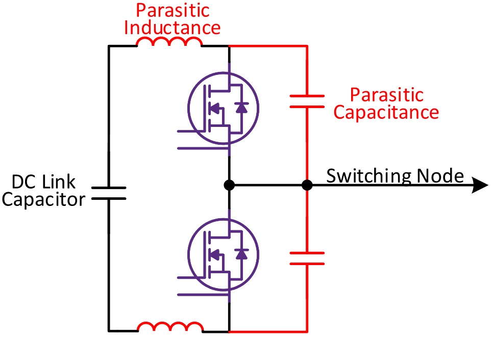
Parasitic inductance can result in several issues depending on the application. Parasitic inductance between the switching devices and the DC bus will increase the voltage overshoot on the device at turn off. Once the PCB layout is complete, the only way to reduce this overshoot is to increase the gate resistor in order to slow down the di/dt of the SiC MOSFET. This will result in increased switching losses. A better solution is to understand and optimize the PCB layout to minimize the parasitic inductance to an acceptable level so that the MOSFET can be driven optimally.
Parasitic capacitance between the switching node and other points in the circuit has the potential to increase switching losses, corrupt signals, and increase EMI. Capacitance between the switching node and the bus rails increases switching losses since the energy stored in the parasitic capacitance is dissipated in the MOSFETs during switching events.
On a multilayer board with complex routing it can be difficult to intuitively visualize all of the parasitic elements and their effect on the circuit operation. If the parasitic elements are not well understood before building a prototype assembly the performance will likely suffer. The warning signs of potential layout issues are:
- High voltage overshoot on turn-off
- Excessive VDS or VGS ringing
- Higher than expected switching losses
- Dynamic current sharing mismatch in parallel devices
Some of these issues can be severe enough to cause immediate device failures or reduce the lifetime of the system. Finding these issues at the prototype stage means that you have already invested significant time and money in ordering, building, testing, and troubleshooting the design only to have to go through the process again with design changes which may or may not be effective. While a SPICE simulator is an effective tool for designing and testing circuit behavior, it doesn’t account for parasitic effects in the layout. That is where a co-simulation tool such as Keysight’s PEPro can be utilized to perform post-layout analysis on the PCB and make design changes before ordering any hardware. PEPro uses an Electromagnetic (EM) field solver to extract PCB layout parasitics. The potential effects noted above can be seen in this type of tool and the layout improved in hours or days compared to months of time invested in building and testing a hardware prototype.
A Case Study – Paralleling MOSFETs
As part of the development process of Wolfspeed’s new evaluation board, KIT-CRD-HB12N-J1, Wolfspeed and Keysight partnered to analyze the design using Keysight ADS and PEPro and comparing the results with measured data in the lab. This effort demonstrates how the Keysight ADS and PEPro simulation tools can be used to predict real-life behavior of a design and use that information to improve the layout.
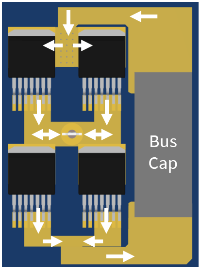
Paralleling discrete SiC MOSFETs allows for increasing the power level of a design up to the 20-60kW level. In order to take full advantage of the parallel MOSFETs, the devices need to switch nearly simultaneously and carry nearly identical current during the on-time so that they have equal power losses. In an ideal system, two MOSFETs would double the amount of power the converter can handle. Any mismatch in losses between the two devices will require the system power to be reduced from that ideal to maintain the same peak Junction Temperature (TJ). Figure 2 shows a symmetrical power path layout for two parallel devices configured in a half-bridge topology which encourages current sharing between parallel devices.
There are a variety of factors that affect the loss and temperature balance between parallel devices. The first one is the parameters of the MOSFET itself (RDS(ON) VGS(TH), etc.) from the natural distribution in the manufacturing process, which the designer has no control over. The range of these parameters is provided in the datasheet and will necessitate some derating of the design to account for potential mismatch between parallel devices. However, the two factors that the designer does have control over, the layout and the cooling system, can have a far larger effect on the performance and balance between parallel devices.
Many SiC MOSFET parameters have a temperature dependence. Even if the electrical layout is perfectly balanced for the parallel devices, the cooling system can introduce imbalance. If the cooling system does not provide equal cooling to all devices due to thermal stacking, flow imbalance, or proximity to other heat sources, the devices will operate at different temperatures. In order to meet reliability requirements, the designer will have to limit the operation of the converter to keep the hottest device within the desired TJ for the application, resulting in underutilization of the other devices.
The PCB layout is the area where a designer has the most control of a design, and consequently the most ability to affect the performance for better or worse. This is the area where Keysight’s PEPro simulation tool can be effective in testing potential layouts, identifying issues, and developing solutions quickly. Wolfspeed’s KIT-CRD-HB12N-J1 is a half-bridge evaluation board with two parallel MOSFETs in each switch position. The board uses a daughter card gate driver. The figures below show the block diagram schematic of the board and an overview of the layout of the power section.
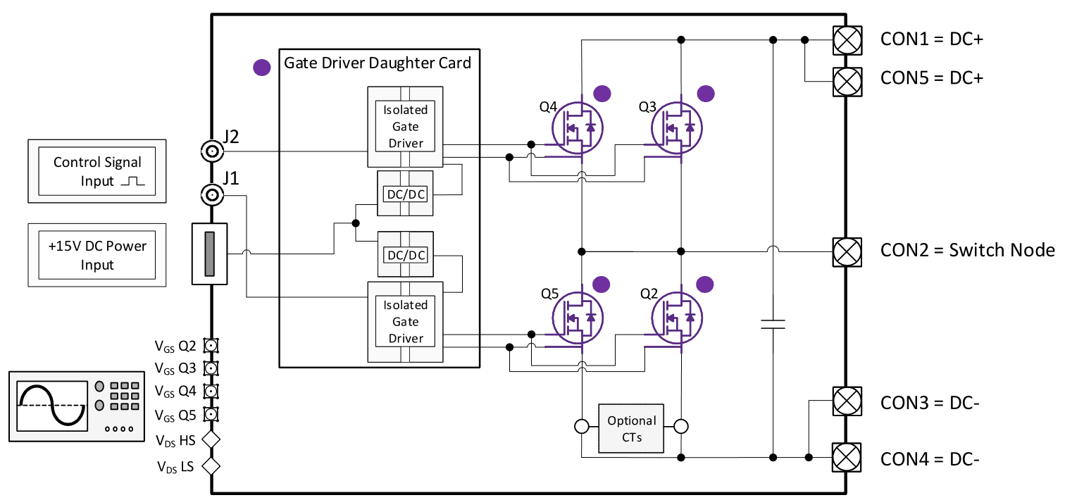
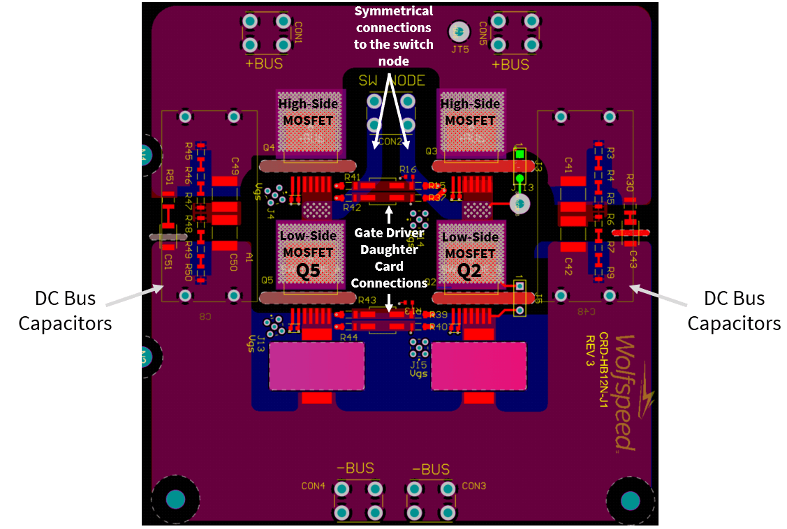
Keysight developed an ADS workspace for the power section of the circuit on this evaluation board. The low-voltage and gate drive circuits were not modeled as part of this exercise since the focus was on symmetry in the power path.
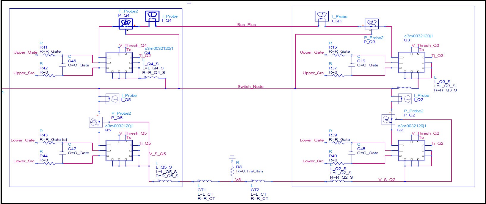
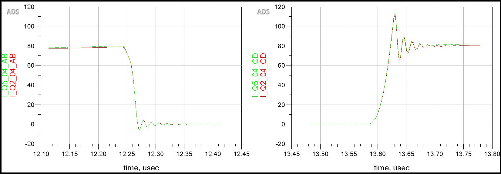
The evaluation board can be used to perform switching loss measurements on the SiC MOSFETs. Each of the parallel MOSFETs has a separate current transducer so that the dynamic current of each device can be analyzed to check for current sharing. If there was an asymmetry in the layout resulting in different parasitic inductance or capacitance at each of the parallel devices, the current at turn-on and turn-off would not match between the two devices. The Keysight simulation shown below shows the current in the two parallel lower SiC MOSFETs. From this simulation it is clear that there is very little mismatch in current between the two devices at the switching edges. This indicates that the layout is very symmetrical for the two devices.
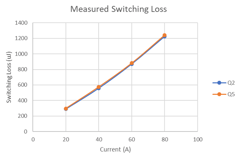
Measured results in the lab confirm that the simulation is correct. The switching losses for these same two devices are nearly identical as shown in the plot below.
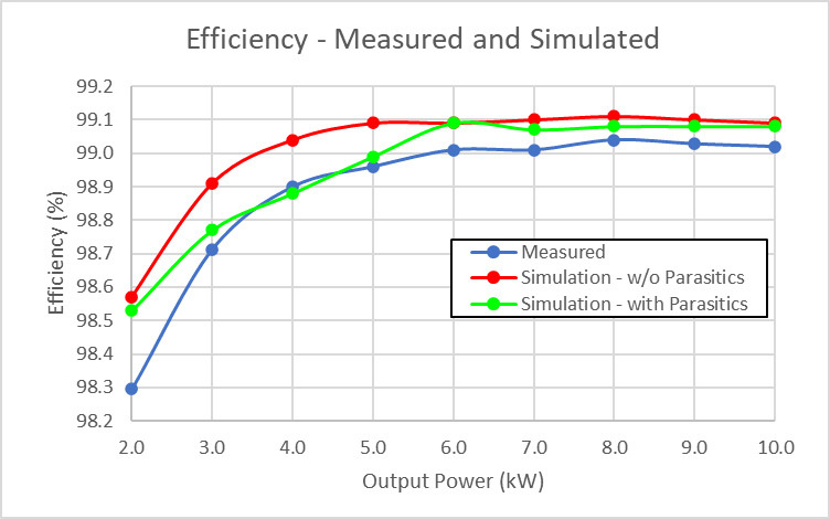
Next, the board was analyzed in the context of running as a synchronous boost converter as shown below.

The efficiency was simulated with and without modeling the parasitic elements of the PCB. The analysis without the parasitic elements included is what a SPICE model alone is capable of. As the plot shows, including the parasitic elements reduces the efficiency and the model is much closer to the measured results seen in the lab. This is an important consideration for designers trying to meet very strict efficiency requirements. The layout can have a significant impact on the losses.
Lastly, an experiment was conducted to intentionally introduce an asymmetry into the design to see the effect on the hardware and the simulation. In the original layout, the switch node connection to the boost inductor was made symmetrically between the two parallel legs. For this test, the connection point was moved to be at the drain tab of Q2, which reduces the resistance and inductance to Q2 and increases it to Q5.
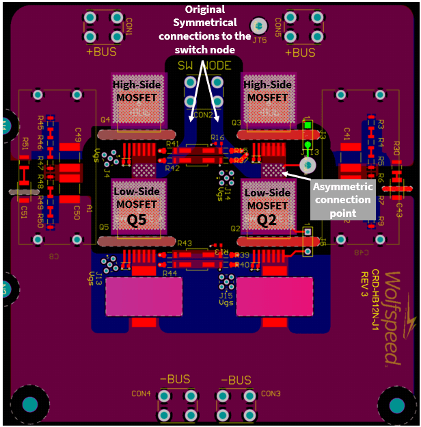
This asymmetry results in increased losses in Q2. The increase in resistance to Q5 causes more of the current to flow through Q2 during the on-time, resulting in higher conduction losses. In the scenario tested, Q5 intentionally had a lower VGS(TH) than Q2, so despite the asymmetry in the layout, Q5 still turns on earlier and takes more of the dynamic current. Keysight ADS is able to capture both phenomenon with good agreement to the measured lab data.

An asymmetry such as this one is often placed into a design to meet other design goals such as location of connection points. However, as Keysight ADS was able to demonstrate, this can have a significant impact on the design performance. Using a tool like this can help a designer to understand all of the tradeoffs in a design and avoid surprises in the testing stage.
Conclusion
Silicon Carbide MOSFETs and diodes have opened the gateway to more efficient and power-dense designs in large part due to their fast switching capabilities. However, with this improvement in switching speeds comes an increased need for designers to be aware of the parasitic elements in a layout that can have a significant impact on the performance. Incorporating electromagnetic modeling with SPICE modeling provides a more complete picture of the behavior of the power converter. These tools can help accelerate design time by avoiding long prototyping cycles and optimize the overall performance of the system.